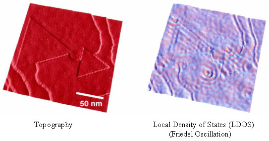
Friedel Oscillations in 2D Electron Gas Systemsat Semiconductor Surfaces The feature of electrons as matter waves, one of the most significant conclusions from quantum mechanics, should be taken into account and controlled to engineering the electron transport in a nanoscale world. We have successfully imaged the electron waves (Friedel Oscillations) by applying a scanning tunneling microscopy (STM) for epitaxially grown semiconductor surfaces. Wavy LDOS patterns due to the electron wave interferences are clearly imaged in the vicinity of an isolated defect and inside of triangle nanostructures.
[ Back ]