Physical Science Laboratory
Aluminum nitride (AlN) has negative electron affinity. Therefore, it is very promising for field emission. Field emission is mainly of interest in its application to field-emission displays, thin flat-panel displays suitable for moving-pictures, and to micro vacuum tubes made of semiconductor microstructures suitable for high-frequency amplifiers. However, the AlN crystal quality reported so far has not been good enough for field emission, and, because the reported AlN was undoped and its free-electron density was low, the reported current density of the field emissions was much lower than that of diamond.
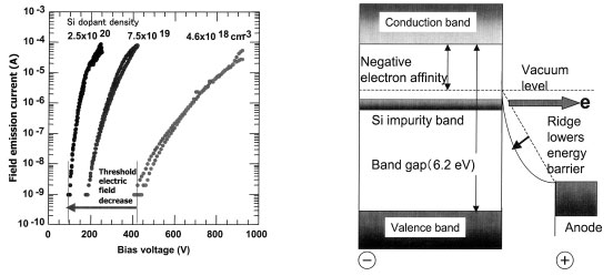
We chose a silicon-carbide (SiC) substrate which has the same lattice constant in plane and the same thermal expansion coefficient as those of AlN. We then grew AlN crystal at 1100oC by MOVPE and this produced AlN crystal of high quality. The full-width at half maximum of the (0002) x-ray rocking curve was less than 100 sec. The value is the narrowest ever, showing that we have grown the best quality AlN. We found that, as the Si dopant density in AlN is increased, the electric field necessary for field emission is decreased as shown in Fig. 1 [1]. The mechanism is shown in Fig. 2. The doped Si supplies the electrons necessary for field emission, and the Si atoms form the impurity level. The electrons are supplied through the impurity band to the surface. Further, we found that ridge structures whose top width is of the nanometer order are formed spontaneously by heavy Si doping (see inside-cover) [2]. The ridge-structure formation lowers the energy barrier necessary for field emission by about 2 eV. As a result, using heavily Si-doped AlN, we have obtained a field-emission current density of 66 mA/cm2, twice that for diamond. In a basic structure for a field emission display, we observed red, green, and blue light from phosphors excited by field-emitted electrons (see inside-cover). Its luminance was 1200 cd/m2, which is intense enough for a practical display.
[1] M. Kasu and N. Kobayashi, Appl. Phys. Lett. 76 (2000) 2910.
[2] M. Kasu and N. Kobayashi, Appl. Phys. Lett. 78 (2001) 1835.
|
|