Device Physics Laboratory
In order to make high performance nanodevices like single-electron devices working at room temperature, nanofabrication at the scale of sub-10 nm is necessary. To enable that, electron beam (EB) nanolithography on inorganic resists has been tried by many groups. The sensitivity of conventional inorganic resists, however, is too low for these resist to be applied to make high-performance nanodevices.
We have developed a new organic/inorganic composite resist that has much higher sensitivity than conventional inorganic resists and sufficient resolution for our purpose. This resist is a chelete compound of a metal alchoxide chemically modified by a b-diketone [1]. EB exposure causes separation of the diketone from the compound, which is followed by spontaneous crosslinkage of the alchoxide. Thus, it can be used as a negative-tone resist to an EB. As the primary reaction due to the EB occurs at the organic ketone part, not at inorganic parts, this resist is more than a hundred times more sensitive to the EB, compared to conventional inorganic resists. The resist enables finer patterning and provides small line-edge roughness due to its structure being as small as a few nanometers.
We have evaluated this resist using our EB nanolithography system at 100-kV acceleration voltage. Besides its small beam size, this system has high stability and reproducibility for sub-10-nm scale lithography. For example, the beam positioning error is less than 2 nm for 10 minutes, and the reproducibility of the stage position is as good as 1-2 nm after 500 stage movements [2].
Figure 1 shows fine lines of the resist exposed to the EB using the system. The width of the lines formed at the center of the main deflection field is about 8 nm. We could also obtain fine lines as narrow as about 10 nm on the boundary of a 320-mm-square mainfield. Good reproducibility and low fluctuation of linewidth are obtained, and the linewidths at the center and the boundary of the field correspond to the diameters of the EB simulated there. These results mean the resist pattern strictly reflects the distribution of the energy absorbed in resist.
[1] M. S. M. Saifullah et al., Jpn. J. Appl. Phys. 38 (1999) 7052.
[2] K. Yamazaki et al., Proc. SPIE. 3997 (2000) 458.
*present address: Engineering Faculty, Cambridge Univ., U.K.
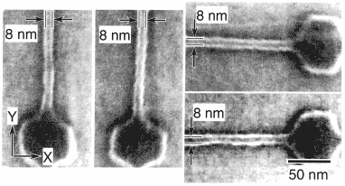
| Fig. 1. | 8-nm-wide lines of composite resist formed at the center of the mainfield. Lines were reproducibly formed with small line edge roughness along both x- and y- axis. |