Physical Science Laboratory
The operational principle of the semiconductor electronic devices fabricated so far is based on the control of the number of electrons passing through the active part of devices. This principle utilizes the feature of electrons as material particles, which had been the excellent description in the classical theory of physics. The recent progress in the semiconductor processing techniques allows the accurate manufacturing of ultimately small devices whose size is in the range of tens of nanometers. In these devices, we need to take into account the other feature of electrons, which is that they act as matter waves. This feature is one of the most significant conclusions drawn from the principle of quantum mechanics. Recently, there have been many device proposals based on novel operational concepts arising from this quantum mechanical feature. To understand the transport phenomena in these kinds of devices in detail, the behavior of electrons as matter waves should be directly observed. From this point of view, we have successfully imaged electron waves in real space by applying low-temperature scanning tunneling microscopy (STM) and our unique crystal growth technique that enables the preparation of an electrically conductive and extremely flat surface of InAs [1,2].
Figure 1 shows local density of states (LDOS) images at a defect scatterer on the InAs surfaces with different electron energies. Wave patterns made up of concentric circles are clearly imaged in the vicinity of the isolated defect. From the nature of oscillation damping, we can conclude that this is the so-called Friedel oscillation due to electrons being laterally scattered by the defect. By observing the bias voltage dependence, the effective mass was estimated to be 0.043 m0, which is in good agreement with previous reports. Our detailed analysis indicates that the observed oscillations are caused by the scattering of the two-dimensional electron gas accumulated in the near-surface region of the InAs surfaces.
[1] H. Yamaguchi et al., Jpn. J. Appl. Phys. 38 (1999) 635.
[2] K. Kanisawa et al., Phy. Rev. Lett. 86 (2001) 3384.
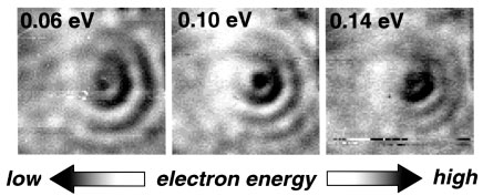
| Fig. 1. | LDOS images in the vicinity of a point scatterer on epitaxially grown InAs (111)A surfaces. |