Materials Science Research Laboratory
Å@Exploration of the spin degree of freedom in addition to the charge degree of freedom is considered to be a key strategy for the realization of new device functions in the future electronics. The research topics that have been pursued thus far from this point of view include (i) the spin injection experiment from a ferromagnetic metal to a semiconductor, (ii) the electric control of the spin precession in a two-dimensional electron gas that is confined in a nonmagnetic semiconductor quantum well (QW), (iii) the magnetic control of electron spins using diluted magnetic semiconductors. Recently, we have proposed a novel spin-filter device that combines the spin-orbit effect due to the built-in electric fields in the heterostructure and a triple barrier resonant tunnel diode [1]. This spin filter, which has almost 100 % spin-filtering efficiency, is unique in a sense that it does not use magnetic properties of materials. This device, therefore, can be fabricated using nonmagnetic semiconductors only. Possible applications of the device include the read-write devices for the information stored in spin qubits or/and magnetic random access memories.
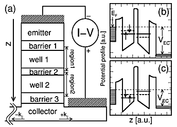
Å@The proposed device consists of a triple barrier structure, where In0.53Ga0.47As
and In0.52Al0.48As are used for
the QWs and the barrier layers, respectively (See Fig. 1). In addition, the
potential profile of the device has a particular mountain-like shape as shown
in Figs. 1(b)(c), which is a result of proper n doping in barriers 1 and 3
and p doping in barrier 2. Because of this particular potential shape, the
resonant tunneling levels that are formed in the first and second QWs (denoted
as wells 1 and 2) experience spin splittings in a way they reflect the positive
and negative electric fields induced within wells 1 and 2, respectively. We
can, then, extract electrons with a specific spin state by adjusting the emitter-collector
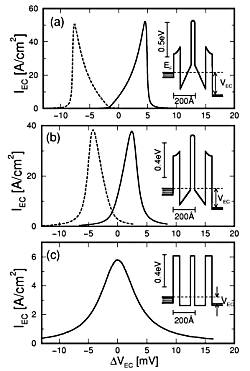
bias voltage VEC properly. Shown in Fig. 2 are the calculated I-V curves of
the proposed device for three different device structures, using the transfer
matrix method. We see that the separation of the spin-split I-V curve peaks
is roughly proportional to the magnitude of the potential slope within the
wells.
[1] T. Koga, J. Nitta, H. Takayanagi, and S. Datta, Phys. Rev. Lett. 88 (2002) 126601.
 |
 |
||||
|
|