Physical Science Laboratory
Å@The recent remarkable progress in fabrication process technologies has enabled the fabrication of nanometer-scale devices. Because electronic properties in the nanometer-scale region are governed by quantum mechanics, the development of quantum devices and quantum computers requires understanding and utilizing the wave phenomena of electrons in nanostructures.
Å@We have measured the local density of states (LDOS) distribution by differential conductance (dI/dV) measurement using scanning tunneling microscopy (STM) at low temperatures [1]. We imaged the electron wave characteristics of conduction electrons, as well as the Friedel oscillation of two-dimensional electron gas (2DEG), at the semiconductor surface of indium arsenide (InAs) thin film.
Å@Using this technique, we imaged the LDOS of zero-dimensional (0D) electron waves confined in a semiconductor nanostructure [2]. Figure 1 shows an STM image and schematic illustration of a semiconductor nanostructure, a so-called stacking fault tetrahedron. We found that when the structure size is comparable to the electron wavelength, the nanostructure behaves as a 0D structure (a quantum dot) and confines 2DEG in the accumulation layer at the InAs surface. We also found that the LDOS distribution of a semiconductor nanostructure coincides with the probability distribution of the 0D eigenstates. Such LDOS distributions are observed at intervals of the 0D level separation. This is because electrons tend to exist at discrete energy levels due to the quantization in the nanostructure. When the electron energy coincides with the quantized levels, quantum mechanical resonance is observed as a higher LDOS in the nanostructure than that in the surroundings.
[1] K. Kanisawa, M. J. Butcher, H. Yamaguchi, and Y. Hirayama, Phys. Rev. Lett. 86 (2001) 3384.
[2] K. Kanisawa, M. J. Butcher, Y. Tokura, H. Yamaguchi, and Y. Hirayama, Phys. Rev. Lett. 87 (2001) 196804.
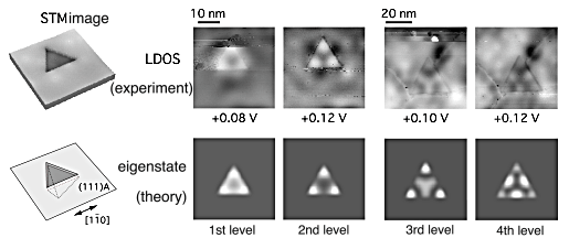
| Fig. 1. | STM image and schematic illustration of nanostructure [left]; LDOS images (experiment) and 0D eigenstates (theory) [right]. Brighter region indicates higher LDOS. |