Materials Science Laboratory
ü@Spin-orbit (S.O.) interaction is an important parameter responsible for the spin precession and spin splitting in semiconductors. Therefore, its control in a semiconductor is considered to be a key for the development of the recently growing research area, "spintronics," where spin degrees of freedom are explored for the realization of new device functionalities [1,2]. The so-called Rashba S.O. interaction (R.S.O.I.) is caused by the structural inversion asymmetry (SIA) in semiconductor heterostructures, of which magnitude is controllable by the applied gate voltages. However, the magnitude of the R.S.O.I. is generally so small that few experimental techniques are readily available for the determination of its magnitude. In this regard, we have been using the weak antilocalization (WAL) analysis successfully, for the first time, for systematic and quantitative evaluation of the strength of the R.S.O.I. [3].
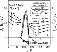
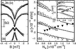
ü@Shown in Fig. 1 are the potential diagrams for the four In0.53Ga0.47As quantum well (QW) samples designed for the present investigation, where carrier supplying layers are introduced both above and below the QW for the systematic control of the QW potential shapes. The results of the magneto-resistance (MR) measurements of these samples at low temperatures (0.3 K) are shown in Fig. 2(a), where we find the weak localization (resistance maximum at zero magnetic field) to WAL (resistance minimum at zero magnetic field) transition as the degree of the SIA increases. Hence, the larger the SIA of the sample, the stronger the S.O. interaction. Shown in Fig. 2(b) are the values of the R.S.O.I. parameter a deduced from the theoretical fitting of the MR data as shown in Fig. 2(a), together with the predicted a values obtained from the küEp perturbation calculations. We see an excellent agreement between the experimental and theoretical a values.
[1] S. Datta and B. Das, Appl. Phys. Lett. 56 (1990) 665.
[2] T. Koga, J. Nitta, H. Takayanagi and S. Datta, Phys. Rev. Lett. 88 (2002) 126601.
[3] T. Koga, J. Nitta, T. Akazaki and H. Takayanagi, Phys. Rev. Lett. 89 (2002) 046801.
 |
 |
||||
|
|