Physical Science Laboratory
(in collaboration with T. Tsuchizawa, T. Watanabe, T. Shoji, and K. Yamada in NTT Microsystem Integration Laboratories)
Å@Photonic crystal having a photonic band gap is expected to one of possible candidates for basic platform of future ultra-small photonic large-scale integrated circuits, and we have been investigating two-dimensional photonic crystals fabricated from SOI (silicon-on-insulator) substrates. We have already realized single-mode waveguides that operate within the photonic band gaps, and demonstrated their exotic dispersion characters [1,2]. The mode size of these waveguides is extraordinarily small, which is one of main reasons why ultrasmall circuits are possible, but it has been pointed out that it is too small to effectively couple the light to ordinary photonic transmission systems, such as optical fibers. In fact, the coupling loss between photonic crystal waveguides and single-mode fibers is larger than 30dB, which is unacceptable for practical application.
Å@To solve this problem, we have realized photonic-crystal waveguides incorporating spot-size converters, in collaboration with NTT Microsystem Integration Laboratories. They are consisting of three parts, namely photonic crystal waveguides, Si-wire waveguides, and polymer waveguides, and the boundaries between these parts have adiabatic spot-size (or mode-profile) converting regions, as shown in Fig. 1. The ultrasmall mode in the photonic crystal waveguide is adiabatically transformed to that in the Si-wire, and then to that in the polymer waveguide that has a spot size comparable to that of a single-mode fiber. We have directly measured and confirmed that the coupling loss of this structure is just 3-4dB, which is far better than that without spot-size converters [3]. This result is a very important step towards future application of photonic crystals, but also important for current research of photonic crystals because it enables us to do various optical measurements which had been practically impossible due to inherent large coupling loss.
Å@
| [1] | M. Notomi et al., Phys. Rev. Lett. 87, (2001) 253902. |
| [2] | M. Notomi et al., IEEE J. Quantum Electron. 38, (2002) 736. |
| [3] | A. Shinya et al., SPIE Photonics West 2003, 5000-21, San Jose, USA. (2003). |
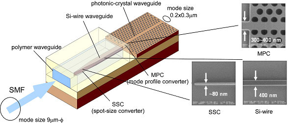
| Fig. 1. | Schematic view of a spot-size conveter for photonic crystal waveguide (left), and electron micrographs of the adiabatic tapers in this device (right). |