Device Physics Laboratory
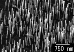
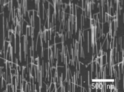
Å@One-dimensional nanomaterials are expected to play a key role in fabricating nanoscale devices of the next generation. However, miniaturization in electronic and optoelectronic devices through improvements in conventional Ågtop-downÅh technologies is approaching the limits of lithographic and etching processes. In contrast, bottom-up approaches to nanodevices, where the nanomaterials are assembled from basic building blocks, such as semiconductor nanowires and carbon nanotubes, have the potential to go far beyond their limits. Recently, we have successfully grown the surface mounted and vertically aligned InP nanowires by metal organic vapor phase epitaxy [1]. The nanowires were grown by the vapor-liquid-solid mechanism with Au nanoparticles acting as the catalyst. The Au nanoparticles were used as the seed to control the nanowire diameter in the nanoscale range. Figure 1 shows a typical scanning electron microscopic (SEM) picture of the nanowires grown on InP(111)B taken at an oblique angle of 40o. Both scanning and transmission electron microscopic studies showed highly dense nanowires with homogeneous diameter along their length axis, and had zinc-blende structure with <111> growth direction, and most of them had diameter in the range of 20 - 25 nm. Photoluminescence measurements at room temperature showed significant blueshift in the peak position compared to bulk InP due to the quantum confinement of the carriers in the nanowires. Furthermore, heteroepitaxial InP nanowires were also successfully grown on GaP(111)B substrates [2]. Figure 2 shows a typical SEM picture of the nanowires grown on GaP(111)B. Highly dense, vertically aligned nanowires with uniform diameters along the vertical axis are visible. Very recently, the site-controlled InP nanowires were successfully grown at the positions where Au nanoparticles have been arranged through liquid Au migration and followed Au nanoparticle formation at a particular position on the patterned Si substarte [3].
[1] S. Bhunia, T. Kawamura, Y. Watanabe, S. Fujikawa, and K. Tokushima,
Appl. Phys. Lett. 83 (2003) 3371.
[2] Y. Watanabe, et al., Proceedings of the Twelfth International Workshop
on the Physics of Semiconductor Devices (IWPSD-2003), Chennai India, December
2003.
[3] Y. Watanabe, et al., Proceedings of Fifth International Workshop on Epitaxial
Semiconductors on Patterned Substrates and Novel Index Surfaces (ESPS-NIS),
Stuttgart Germany, October 2003.
 |
 |
||||
|
|