Physical Science Laboratory
ü@At present the data transfer rate in communications is increasing very rapidly.
Therefore, electronic devices that can operate at higher frequencies with
higher output power are eagerly needed. Diamond has the highest thermal conductivity
among materials and therefore offers the highest heat dissipation efficiency
during high-power operation. Diamond exhibits a very high breakdown electric
field, which means diamond devices can operate at extremely high voltage.
These properties are important for high-output-power devices. In addition,
the carriers in diamond have a high mobility and a high saturation drift velocity,
which make high-frequency and high-speed operation possible. In fact, from
device figures of merit calculated from the physical properties of high-frequency
high-power devices diamond is the best among semiconductors and can therefore
be called ügultimate semiconductor.üh However, until now, the growth of high-quality
diamond thin film had been impossible because of the formation of numerous
crystalline defects and impurities during growth.
ü@We have developed a CVD growth technology for high-quality diamond thin films
with a low density of defects and impurities [1] and, using those thin films,
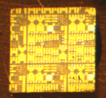
have, in collaboration with the University of Ulm, Germany, fabricated diamond
field-effect transistors (FET) [2], as shown in Fig. 1. In the FET, a quasi
two-dimensional hole channel formed as a result of hydrogen surface termination,
and we formed a 0.2 ā╩m-long short gate contact using electron-beam lithography
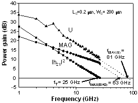
and self-aligned technology. As shown in the frequency dependence of power
gains (Fig. 2), the FET exhibited the transition frequency (fT)
for |h21|2 of 25 GHz, and the maximum oscillation frequency
(fMAX) for the maximum available gain (MAG) and unilateral power
gain (U) of 63 and 81 GHz, respectively. These values are the highest ever
for diamond, and show the first amplification in the millimeter-wave range.
ü@The power characteristics of the diamond FET for A-class operation at 1 GHz
showed a linear power gain of 14 dB for a wide input power range, and the
maximum output power (PMAX) of 0.35 W/mm. The PMAX is
the highest ever for diamond, and will be increased by one order by optimizing
the device structure. The microwave noise measurements of the FET showed that
the minimum noise figure (Fmin) was only 0.72 dB at 3 GHz. This
Fmin is better than that of Si MOSFET and comparable with those
of p-GaAs HEMT and n-GaN HEMT with the same gate length. This means that a
diamond FET is very promising for microwave receivers as well as transmitters.
ü@
| [1] | M. Kasu, M. Kubovic, et al., Diamond and Related Materials 13 (2004) 226. |
| [2] | M. Kubovic, M. Kasu, et al., to be published in Diamond and Related Materials (2004). |
 |
 |
||||
|
|