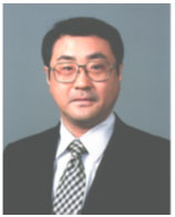
Toshiki Makimoto was born in Tokyo on January 16, 1960. He received the B.E., M.S. and Ph.D. degrees in electrical engineering from the University of Tokyo in 1983, 1985 and 1993, respectively. He joined NTT Basic Research Laboratories in 1985. He was a visiting researcher in University of California, Santa Barbara, USA during 1993-1994. Since 1985, he has engaged in epitaxial growth of III-V compound semiconductors, in-situ monitoring of epitaxial growth, heterojunction bipolar transistors, and so on. His current interests are epitaxial growth of nitride semiconductors and its application to devices. He is a member of technology evaluation committee for the New Energy and Industrial Technology Development Organization (NEDO) and the Diamond Research Center in the National Institute of Advanced Industrial Science and Technology (AIST). He is an associate editor of Japan Society Applied Physics International and a member of the Japan Society of Applied Physics, and the Institute of Electronics, Information and Communication Engineers.
Distinguished Technical Member

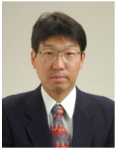
Hiroshi Yamaguchi was born in Osaka on October 30, 1961. He received the B.E., M.S. in physics and Ph.D. degrees in engineering from the Osaka University in 1984, 1986 and 1993, respectively. He joined NTT Basic Research Laboratories in 1986. He was a visiting research fellow in Imperial College, University of London, UK during 1995-1996. Since 1986 he has engaged in the study of compound semiconductor surfaces prepared by molecular beam epitaxy mainly using electron diffraction and scanning tunneling microscopy. His current interests are mechanical and elastic properties of semiconductor low dimensional structures. He is a research coordinator of NEDO international joint research project (Nano-elasticity) during 2001-2004 and a member of the Japan Society of Applied Physics and the Physical Society of Japan. He was awarded the paper awards of the Japanese Society of Applied Physics in 1989 and 2004.
Distinguished Technical Member

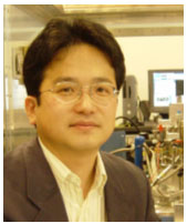
Toshimasa Fujisawa was born in Tokyo on May 23, 1963. He received the B.E., M.S. and Ph.D. degrees in electrical engineering from Tokyo Institute of Technology in 1986, 1988 and 1991, respectively. He joined NTT Basic Research Laboratories in 1991. He was a guest scientist in Delft University of Technology, Delft, the Netherlands during 1997-1998. Since 2003, he is also a guest associate professor at Tokyo Institute of Technology. Since 1991 he has engaged in the study of semiconductor fine structures fabricated by focused-ion-beam technique and electron-beam lithography technique, transport characteristics of semiconductor quantum dot. His current interests are single-electron dynamics in quantum dots, and their application to quantum information technologies. He received Sir Martin Wood Prize in 2003 and JSPS (Japan Society for the Promotion of Science) Award in 2005. He is a member of the Japan Society of Applied Physics, and the Physical Society of Japan.
Distinguished Technical Member

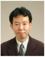
Masaya Notomi was born in Kumamoto, Japan, on 16 February 1964. He received his B.E., M.E. and Dr. Eng. degrees in applied physics from University of Tokyo, Tokyo, Japan in 1986, 1988, and 1997, respectively. In 1988, he joined Nippon Telegraph and Telephone Corporation, NTT Optoelectronics Laboratories, Atsugi, Japan. Since then, his research interest has been to control the optical properties of materials and devices by using artificial nanostructures, and engaged in research on semiconductor quantum wires/dots and photonic crystal structures. He has been in NTT Basic Research Laboratories since 1999, and is currently working on light-propagation control by use of various types of photonic crystals. From 1996-1997, he was with Linkö;ping University in Sweden as a visiting researcher. He is also a guest associate professor of Tokyo Institute of Technology (2003- ). He is a member of the Japan Society of Applied Physics, and the American Physical Society.