Kazuhide Kumakura, *Masanobu Hiroki, and Toshiki Makimoto
Materials Science Laboratory, *NTT Photonics Laboratories
Å@The quality of a GaN layer grown on sapphire substrates
by metalorganic vapor phase epitaxy (MOVPE) has been improved by the use of
low-temperature AlN or GaN buffer layers. Since the low-temperature deposited
layer is unstable, it is well-known that variously shaped islands were formed
as temperature increased. Therefore, it is difficult to grow the GaN layer
with sufficient quality or reproducibility, which is a quite severe problem
from the commercial point of view. Thus, it is important to find a new buffer
layer for GaN growth on sapphire substrates.
Å@Electron cyclotron resonance (ECR) plasma sputtering can easily deposit a
minute, uniform, and stable oxide or nitride layer on large area at room temperature.
An Al2O3 and an AlN can also be easily deposited by
ECR plasma sputtering at room temperature, and have very high melting points
above 2000Åé, indicating that these materials could be used as a buffer layer
with good thermal stability. Therefore, we have proposed and demonstrated
the GaN growth on sapphire substrates with the ECR plasma sputtered layer
of Al2O3/graded-AlON/AlN/Al2O3
as a buffer layer instead of low-temperature AlN or GaN layer.
Å@We formed the buffer layers on c-face sapphire substrates by ECR plasma sputtering
at room temperature and used them as the growth substrates. The total thickness
of the buffer layers was 20 nm. We directly grew GaN on these substrates at
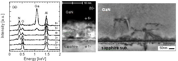
1000Åé. Figures 1 (a) and (b) show the energy dispersion x-ray spectroscopy
(EDS) profiles and the cross-sectional transmission electron microscope (TEM)
image at the interface between the sapphire substrate and the GaN layer, respectively.
The peak intensities from nitrogen (N) increased gradually from the sapphire
substrate to GaN layer, and those from oxygen (O) decreased gradually, as
shown in Fig. 1 (a). These results indicate that we can easily form the nitride
layer by gradually changing the composition from the oxide layer.
Å@The cross-sectional bright-field TEM image showed that the dislocations were
bended at the initial stage of the growth as shown in Fig. 2, which indicated
the enhancement of the lateral growth, resulting in the decrease of dislocation
density to be 6.0 Å~ 108 cm-2 in the GaN layer. The mobility
of the GaN layer was 540 cm2/VÅEs at the electron concentration
of 2 Å~ 1017 cm-3. These results indicate that the quality
of the GaN layer grown using the ECR plasma sputtered buffer was comparable
or superior to the conventional grown GaN using the low temperature buffer
layer.
 |
||
Figs. 1.
(a) The EDS profiles and (b) the cross-sectional TEM image at the
interface between the sapphire substrate and the GaN layer, respectively.
|
Fig. 2. Cross-sectional TEM image of the interface between the sapphire substrate and GaN layer. | |