Tomoaki Kawamura, Satyaban Bhunia, *Seiji Fujikawa and Yoshio Watanabe
Material Science Laboratory, *University of Hyogo
Å@Nanowires composed of several semiconductor materials have recently been
attracting many interests due to their promising potential for nano-technology
applications such as photonics, quantum computing and bio / medical engineering.
Several nanowires have been grown using the vapor-liquid-solid (VLS) mechanism
in a gaseous environment and evaluated after the growth, using electron-based
microscopic techniques, such as SEM and TEM. Since electron-based techniques
are limited in vacuum, usual monitoring tool, for example, RHEED and LEED
can not be applied to observe nanowire growth, and details of the growth is
still unclear. In contrast with the electrons, x-ray has larger permeability
with the materials, and is often used for monitoring crystal growth in solid,
liquid and gases.
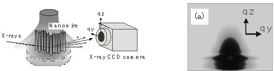
Å@In this work, we evaluated nanowire growth with using GISAXS (Grazing Incidence
Small Angle X-ray Scattering) since this technique can be applied fro evaluating
nano-structures in a gaseous and liquid environment. Figure 1 shows the experimental
layout for GISAXS measurement. X-rays were impinged at the grazing condition
and scatterings from the nanowires were observed with the digital x-ray CCD
camera every several seconds. Figure 2 shows the GISAXS image obtained just
after the nanowire growth. Obviously, clear scatterings along qy and qz direction
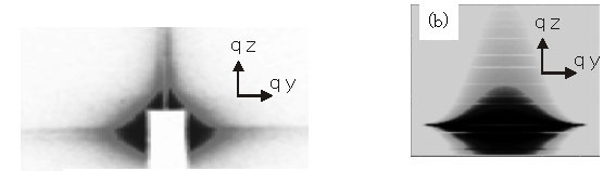
were observed, suggesting dense nanowires on the substrate. Theoretical calculations
with using DWBA (Distorted Wave Born Approximation), shown in Fig. 3 (a) and
(b), suggests x-rays were scattered mainly by the hexagonal objects than hemispheres.
This was consistent with the results of SEM observation which clearly showed
vertical nanowires with hexagonal cross-section.
[1] T. Kawamura, et al., Proc. of XTOP 2004, Prague, September 2004.
[2] S. Bhunia, et al., Appl. Phys. Lett. 83 (2003) 3371.
 |
|||
| Fig.1 Experimental
layout of GISAXS. |
|||
 |
|||
| Fig.2 GISAXS image after
nanowires formation (Ts=400Åé) |
Fig.3 Calculated GISAXS
image by DWBA approximation. (a) hemisphere, (b) hexagonal pillar. |
||