Å@
Tetsuya Akasaka, Yasuyuki Kobayashi and Toshiki Makimoto
Materials Science Laboratory
Å@Sapphire is attractive for a substrate of GaN growth, because it is inexpensive and has a large area, compared with alternatives, such as SiC and GaN substrates. However, a large number of crystal defects (threading dislocations) are formed in GaN films because of the large mismatches in the lattice constants and thermal expansion coefficients between GaN and sapphire. In addition, GaN films grown on sapphire generally contain many residual carriers and have low carrier mobilities. The techniques normally used to reduce crystal defects in GaN or improve its electronic properties are complicated. A novel simple method that can solve these problems simultaneously is therefore highly desired. We have obtained GaN films with low threading dislocation density (TDD) as well as with few residual carriers and high mobility using BGaN micro-islands as novel buffers for the first time [1].
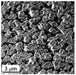
Å@The BGaN (B~2%) formed micro-islands as shown in Fig. 1, because BGaN
caused the phase separation due to the low solubility of B atoms in GaN.
Such a three-dimensional structure is not favorable for device application.
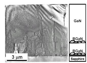
However, epitaxial lateral overgrowth (ELO) of a GaN film on the BGaN micro-islands
resulted in the smooth and continuous surface. Figure 2 shows a cross-sectional
transmission electron micrograph (X-TEM) for a GaN film grown using double
layers of BGaN micro-islands. ELO of GaN reduced the TDD by two orders
of magnitude and the TDD near the GaN surface became 2x108 cm-2. Threading dislocations were annihilated by bending and lateral propagation
and by the formation of half-loops and fused dislocations. We confirmed
that the residual carrier concentration in the GaN film was very low. Using
BGaN micro-islands, we fabricated an AlGaN/AlN/GaN heterostructure, which
is a basic component of GaN-based transistors. This heterostructure exhibited
two-dimensional electron gas mobility of 1910 cm2/Vs at room temperature, which is among the highest ever reported for heterostructures
on sapphire.
Å@The present technique can grow GaN films with smooth surfaces, low TDD, and excellent electronic properties on sapphire in just a single crystal growth process. Therefore, it is very promising as a core technology for reducing the fabrication costs and prolonging the lifetimes of GaN-based transistors and light emitting devices.
[1] T. Akasaka and T. Makimoto, Jpn. J. Appl. Phys. (JJAP Express Letter) 44 (2005) L1506.
 |
 |
|||||
|
Å@Å@ |
|
||||