Å@
Kenji Yamazaki and Hideo Namatsu*
Physical Science Laboratory
Å@Creating three-dimensional (3D) structures with resolutions on the order of nanometers (i.e., 3D-nanofabrication) has been focused for various nanotechnology applications such as NEMS (nano-electromechanical systems). We have already achieved 3D nanofabrication/ nanopatterning of resist material using electron beam lithography (EBL) and obtained a resolution as high as 10 nm and reasonable speed [1]. We have recently succeeded in developing a new resist-coating technique that enable us to apply the 3D technique to various materials. In addition, we obtained good results on patterning and etching of a 3D-resist-coated Si cube.
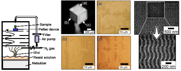
Å@Figure 1 shows the setup for our resist-coating technique. The ultrasonic
nebulizer produces a mist of resist solution, and only fine particles in
the mist are transported to the sample chamber using N2 gas, resulting in quasi static ambient of very fine mist there. Coating
PMMA (polymethylmethacrylate) resist on a Si cube of 1 mm was investigated.
We found that the solvent of the resist solution, the temperature of the
sample, and the flow rate of the transportation gas are important factors
for uniformly coating resist with small surface roughness on each face.
For example, we found that methyl isobutyl ketone, which has lower solubility
for PMMA and thus provides smaller surface/interface energy, is a good
solvent, and that careful adjustment of the temperature to around the dew
point resulting in a thin film of resist solution on the substrate. Errors
of less than 50-60% in resist film thickness among faces and within a face
were obtained after optimizing the conditions [2]. Figure 2 (left) shows
the patterns delineated by EBL on different faces of a Si cube. It is clear
that similar patterns were fabricated on each face. Moreover, the patterns
were transferred to SiO2 layer by dry etching, and the resulting micrograph [Fig. 2 (right)] shows
a resolution 50 nm or less.
Å@This resist-coating technique enables us to coat resist on various 3D substrates, and thus makes possible 3D nanofabrication with a high degree of freedom, combined with 3D EBL and etching. Therefore, it promises to become a key technique for 3D nanotechnology.
[1] K. Yamazaki et al., Jpn. J. Appl. Phys. 43 (2004) L1111-L1113.
[2] K. Yamazaki and H. Namatsu, Tech. Digest 19th IEEE Conf. MEMS (2006) 254-257.
[3] K. Yamazaki and H. Namatsu, Jpn. J. Appl. Phys. 45 (2006) L403-L405.
*Present address: NTT-AT
 |
||||||
|
Å@Å@ |
|
||||