Å@
Tetsuya Mukai1, Alexander Kasper1 and Fujio Shimizu2
1Physical Science Laboratory
2University of Electro-Communications/NTT Research Professor
Å@Neutral atoms have specific features suitable for realizing quantum computers/gates,
e.g. quantized internal states, indistinguishability, controllability of
the atom-atom and atom-photon interactions, and very small influence from
the environment. A promising approach is using a pair of internal states
of the atom as a unit of quantum computation (qubit). To realize this "internal-state-qubit",
making confinement of single atoms in 2- or 3-dimensional arrays will be
a key technique. In the world of atom optics experiments, making single
atom traps is a challenging job because of the influence from a surface
and current noise.
Å@We are trying to achieve the atomic arrays with two different approaches:
using lasers to form an optical lattice (3D) and employing magnetic micro
traps formed by wires, i.e. atom chip (2D). With the optical lattice approach,
we have two original schemes: (i) double optical lattices [1], which is
using two different atomic species trapped in independent optical lattices
with the same lattice constant, and (ii) an all optically controlled "lattice-in-cavity",
which uses a cavity mode as a bus for all qubits. With these methods we
will be able to achieve a universal set of gates with more than 1,000 qubits.
Å@The atom chip approach is using our fine processing technique for making
a 2-dimensional array of atoms. An advantage of the atom chip, which is
not possible with optical lattices, is that we can control and address
specific lattice sites, which is essential for future applications. Our
approach in addition allows us to overcome for example current noise problem
by using superconducting materials. We have constructed an apparatus combining
two functions: a flux cryostat to cool a superconducting atom chip (Fig.1)
and a laser/magnetic trap system to pre cool and trap atoms. With this
apparatus we have for the first time demonstrated the trapping of atoms
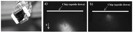
with magnetic potential generated by a superconducting current. Figure
2 represents the absorption images of atoms (a) before and (b) after trapping
with a magnetic potential (the brighter represents the higher atomic density).
With this superconducting atom chip technique we are going to make single
atom traps in the vicinity of a surface as a resource for quantum computations.
[1] F. Shimizu, Jpn. J. Appl. Phys. 43 (2004) 8376.
 |
||||||
|
Å@Å@ |
|
||||