 |
 |
 |
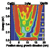
| Scanning tunneling spectroscopy on cleaved semiconductor heterostructure surfaces | Quantized subbands in a quantum well |
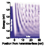
Electron wave interference at a potential barrier |
|
|
|
| Scanning tunneling spectroscopy on cleaved semiconductor heterostructure surfaces | Quantized subbands in a quantum well |
Electron wave interference at a potential barrier |
Å@Å@
Density-of-states Imaging in Semiconductor Heterostructures
Å@
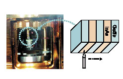
We have succeeded in the spatial imaging of the density-of-states (corresponding to the squared wavefunctions) in semiconductor heterostructures by scanning tunneling spectroscopy on cleaved surfaces. Quantized subbands in a quantum well, electron wave interference at a potential barrier, and wavefunction coupling in a double quantum well have been clearly observed. This method makes it possible to analyze wavefunction distributions in optical and electronic heterostructure devices. (Page 33)
[back]Å@[Top]Å@[Next]