Å@
Haruki Sanada, Hideki Gotoh, Kouta Tateno, Tetsuomi Sogawa, and Hidetoshi Nakano
Optical Science Laboratory
Å@Semiconductor nanowires (NWs) have been extensively investigated as fascinating
candidates for nanoscale photonics and electronics applications. The vapor-liquid-solid
(VLS) method is a technique for fabricating freestanding NWs with a broad
range of semiconductor materials. The method not only produces one-dimensional
structures, but also offers additional flexibility as regards band structure
engineering by employing a conventional heterostructure technology. Here
we report the results of an experimental photoluminescence (PL) measurement
undertaken to clarify the optical properties of single GaAs quantum dots
(QDs) formed in (Al,Ga)As NWs grown by the VLS method [1].
Å@We fabricated GaAs QDs in (Al,Ga)As NW by the following two steps: (1)
VLS growth of the NWs that have GaAs/(Al,Ga)As heterojunctions; and (2)
normal MOVPE for covering the NWs with (Al,Ga)As cap layers, which suppress
the non-radiative surface recombination of photoexcited carriers [2]. Figure
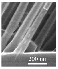
1 shows a cross-sectional SEM image of the similar structure composed of
a GaAs/AlAs system instead of a GaAs/(Al,Ga)As system. The image shows
that several QDs have formed inside the NW.
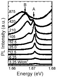
Å@In Fig. 2, we compare the PL spectra with different excitation powers
(Pexc) to examine the characteristics of the two peaks
labeled by A and B. For Pexc
< 100 W/cm2, the integrated intensities of peak A and B have linear dependence with
Pexc and Pexc2, respectively, which is a typical behavior of exciton and biexciton emissions.
In addition, the biexciton peak (peak B) energy exhibits a red shift and
its linewidth broadens as Pexc
increases. This might be a characteristic of QDs in NW structures grown by the VLS
method because similar features have been reported in VLS-based InAs/GaAs and
Ga(As,P)/GaP QDs systems. We also found that the PL depends on the optical
polarization axis, indicating that the nanostructures have a highly
asymmetrical shape. Although a more explicit consideration of their structural
configurations is required to clarify the mechanism, our method is a promising
way of engineering the positions and optical properties of GaAs/(Al,Ga)As
nanostructures.
[1] H. Sanada, H. Gotoh, K. Tateno, and H. Nakano, Jpn. J. Appl. Phys.
46 (2007) 2578.
[2] K. Tateno, H. Gotoh, and Y. Watanabe, Appl. Phys. Lett. 85 (2004) 1808.
 |
 |
|||||
|
Å@Å@ |
|