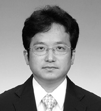
Toshimasa Fujisawa was born in Tokyo on May 23, 1963. He received the B.E., M.S. and Ph.D. degrees in electrical engineering from Tokyo Institute of Technology in 1986, 1988 and 1991, respectively. He joined NTT Basic Research Laboratories in 1991. He was a guest scientist in Delft University of Technology, Delft, the Netherlands during 1997-1998. Since 2003, he is also a guest associate professor in Tokyo Institute of Technology. Since 1991 he has engaged in the study of semiconductor fine structures fabricated by focused-ion-beam technique and electron-beam lithography technique, transport characteristics of semiconductor quantum dot. His current interests are single-electron dynamics in quantum dots and their application to quantum information technologies. He received Sir Martin Wood Prize in 2003 and JSPS (Japan Society for the Promotion of Science) Award in 2005. He is a member of the Japan Society of Applied Physics, and the Physical Society of Japan.
Distinguished Technical Member

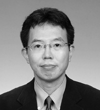
Masaya Notomi was born in Kumamoto, Japan, on 16 February 1964. He received his B.E., M.E. and Dr. Eng. degrees in applied physics from The University of Tokyo, Japan in 1986, 1988, and 1997, respectively. In 1988, he joined NTT Optoelectronics Laboratories. Since then, his research interest has been to control the optical properties of materials and devices by using artificial nanostructures, and engaged in research on semiconductor quantum wires/dots and photonic crystal structures. He has been in NTT Basic Research Laboratories since 1999, and is currently working on light-propagation control by using various types of photonic crystals. During 1996-1997, he worked for Linkping University in Sweden as a visiting researcher. He is also a guest associate professor in Tokyo Institute of Technology (2003- ). He received 2006/2007 IEEE/LEOS Distinguished Lecturer Award. He is a member of the Japan Society of Applied Physics, the American Physical Society, and IEEE/LEOS.
Distinguished Technical Member

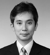
Akira Fujiwara was born in Tokyo, Japan on March 9, 1967. He received his B.S., M.S., and Ph.D. degrees in applied physics from The University of Tokyo, Japan, in 1989, 1991, and 1994, respectively. In 1994, he joined the LSI Laboratories, Nippon Telegraph and Telephone (NTT) Corporation, Kanagawa, Japan. He moved to the Basic Research Laboratories (BRL) in 1996. Since 1994, he has been engaged in research on silicon nanostructures and their application to single-electron devices. He was a guest researcher at the National Institute of Standards and Technology (NIST), Gaithersburg, MD, USA during 2003-2004. He received the SSDM Young Researcher Award in 1998, SSDM Paper Award in 1999, and Japanese Journal of Applied Physics (JJAP) Paper Awards in 2003 and 2006. He was also awarded the Young Scientist Award from the Minister of MEXT (Ministry of Education, Culture, Sports, Science, and Technology) in 2006. He is a member of the Japan Society of Applied Physics and the IEEE.