Å@
1Physical Science Laboratory, 2Delft University of Technology
Å@Å@Nanoelectromechanical systems (NEMS) are attracting much interest as
sensors with very high sensitivities and as new-principle devices. Our
group has reported mechanical systems using InAs/AlGaSb heterostructures
and sensitivity enhancement using quantum effects on electrons in the structures.
However, the basic mechanism of piezoresistance (i.e., resistance change
due to mechanical strain) in such systems has not been understood well.
In this study, we fabricated InAs/AlGaSb NEMS and measured/analyzed its
piezoresistance. The results strongly imply that the piezoresistance in
such systems is significantly affected by the piezoelectric effect and
thus reveale, for the first time, the importance of the piezoelectric effect
in mechanical systems using very thin heterostructures.
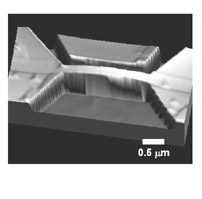
Å@Å@Figure 1 shows an atomic force microscopy (AFM) image of a fabricated
double-clamped nanobeam made of an InAs/AlGaSb heterostructure. The thicknesses
of InAs and AlGaSb layers are 15 and 35 nm, respectively. Depending on
the depth of wet etching, which makes the nanobeam suspended, the shape
of the beam becomes straight or arched. This is because the shear stress
due to the lattice mismatch curls the wide suspended supports upward, and
the beam linking the two supports thus becomes arched. The piezoresistance
measured using an AFM tip for deflecting the beam had large dependence
on the beam shape. That is, the gauge factor (GF) derived from the resistance
change and strain, which usually reflects material properties, was positive
or negative depending on whether the beam was straight or arched, and the
magnitude was much larger than for bulk (See Table) [1]. To try to understand
these surprising phenomena, we calculated the piezoresistance, including
the piezoelectric effect (Fig. 2). The results suggest that the piezoresistance
is significantly affected by the piezoelectric effect for heterostructure
thin film. That is, additional charges on the beam surface, which are induced
by the piezoelectric effect when the structure is strained, change the
resistance, and this effect is larger when the conductive layer is thinner
and thus the carrier density is lower. Moreover, the opposite signs were
also obtained for the arched and straight beams by calculation, which means
that our understanding roughly explains the experimental results.
Å@Å@These results enhance our understanding of piezoresistance in NEMS,
which could lead to more effective designs for them.
Å@Å@This work was supported in part by Japan Society for the Promotion
of Science (JSPS) KAKENHI(16206003) and the Dutch NWO VICI-grant.
[1] K. Yamazaki, S. Etaki, H. S. J. van der Zant, and H. Yamaguchi, J. Cryst. Growth 301-302 (2007) 897.
 |
Å@ | 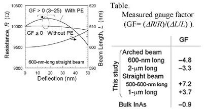 |
||||
|
|