Å@
1Physical Science Laboratory, 2LPN-CNRS
Å@Å@One of the advantages of two-dimensional electron system (2DES) formed
in semiconductor heterostructures is the possibility to control the main
system parameters, including electron confinement tuned by varying the
thickness of the grown layers and electron density tuned by applying an
external electric field. Recently, we found that the Fermi level was mostly
unpinned at the (111)A clean surface of n-type In0.53Ga0.47As [1]. Therefore, it could be possible to vary the electron density in
the (111)A-oriented In0.53Ga0.47As surface quantum well (QW) to access 2DES by using scanning tunneling
spectroscopy (STS) measurements in the ultra-high vacuum (UHV). This allows
us to perform studies of electron phenomena in disordered 2DES at the nanometer-scale
spatial resolution. The effect of disorder is very important to understand
various electron behaviors, especially the many-body phenomena in the semiconductor
structures.
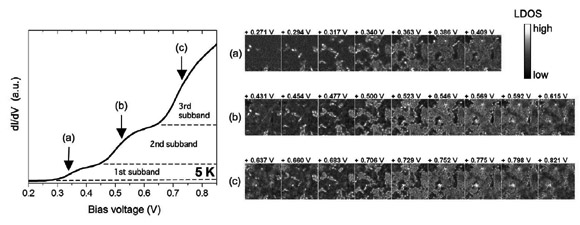
Å@Å@An In0.53Ga0.47As/In0.52Al0.48As multi-subband surface QW was grown by molecular beam epitaxy on lattice-matched
InP(111)A substrate, and the electronic local density of states (LDOS)
in this QW was measured at 5 K by low-temperature STS in UHV. The LDOS
in the conduction band has a clear step-like energy dependence, revealing
that 2DES subbands are formed in the QW (Fig. 1). At a given energy, the
LDOS shows strong spatial fluctuations in the QW plane due to the presence
of a disorder potential. The formation of the localized states is due to
quantum-mechanical interference between electron waves that have undergone
multiple scatterings by the disorder potential. Percolation of localized
states with increasing energy is observed in each subband tail. This percolation
is explained by using a semiclassical model. The origin of the disorder
potential is ascribed to a random distribution of native point defects
located at the QW surface [2].
Å@Å@This work was partly supported by a Grant-in-Aid for Scientific Research
from the Japan Society for the Promotion of Science, JSPS KAKENHI (16206003).
[1] S. Perraud, et al., Appl. Phys. Lett. 89 (2006) 192110.
[2] S. Perraud, et al., Phys. Rev. B 76 (2007) 195333.
 |
||
|