ü@
Optical Science Laboratory
ü@ü@Recently, nanowires (NWs) have become the center of attention due to
the exceptional versatility and promise a wide range of potential applications,
from electronics and photonics to biochemistry and medicine [1]. Semiconductor
NWs are expected to play an important role as functional device elements
in nanoscale electronic devices. InAs NWs are very promising for high-speed
device applications due to their high mobility. We have established a reproducible
fabrication process for NW field effect transistors (FETs) and the performance
of the InAs NW-channel FETs were evaluated [2].
ü@ü@Au colloidal particles were used as the catalyst for the growth of
InAs NWs by vapor-liquid-solid mode in a low-pressure (76 Torr) metalorganic
vapor phase epitaxy system [3]. The precursors were trimethyl-indium and
AsH3. Transmission electron microscopy measurement indicates that the NWs are
wurtzite-structure without stacking faults. The NWs were dispersed on a
SiO2/Si (SiO2 thickness: 500 nm) substrate and then Ni/Au metals were selectively deposited
on the NWs to form electrical contacts after patterning by electron beam
lithography. The contacts were annealed at 300 üÄ for 30 s by rapid thermal
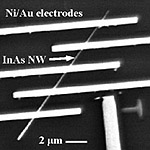
processing. Figure 1 shows a NW-channel FET with a number of electrodes.
ü@ü@Using the underlying heavily doped Si substrate as the gate electrode,
we measured the DC characteristics of InAs NW-channel FETs with a semiconductor
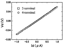
parameter analyzer at room temperature. Figure 2 shows typical characteristics
of Id-Vd of 2 and 4-terminal measurements. Compared with NW resistance, the contact
resistance is very small and the specific contact resistivity is estimated
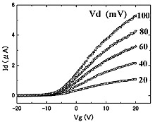
to be 2.0ü~10-7 āČcm2. Figure 3 shows typical Id-Vg characteristics at different drain voltages. The feature that the current
increases with the gate voltage indicates that the NW is n-type. The NW-channel
FETs show a maximum transconductance (gm) in the range of 0.24-0.36 µS at Vd of 0.1 V. For FET devices, the normalized transconductance g*m = gm/wg is an important figure of merit, where wg is the channel width (in the case of NW channel, the width is the NW diameter).
The g*m varies in the range of 2.5-3.7 mS/mm at Vd of 0.1 V. Based on the FET properties, the electron concentration (N) and mobility (µ) of the NW segment could be estimated. N and µ are in the range of 2.3-5.8ü~1017 cm-3 and 1.29-1.53ü~103 cm2V-1 s-1, respectively. We are investigating how to further improve the FET properties
and fabricate functional quantum devices.
ü@ü@This work was partly supported by JSPS-KAKENHI (16206003, 18310074).
[1] Y. Li, et al., Mater. Today 9(10) (2006) 18; C. Thelander, et al., ibid. 9(10) (2006) 28; P. J. Pauzauskie and P. Yang, ibid. 9(10) (2006) 36.
[2] G. Zhang, et al., ISCS2007, Kyoto, Japan, Oct. 2007, p. 142.
[3] G. Zhang, et al., J. Appl. Phys. 103 (2008) 014301.
 |
 |
 |
||||||||
|
|
|