Physical Science Laboratory, *Materials Science Laboratory
Graphene has recently attracted much attention due to its superior electric
properties. Epitaxial graphene grown on SiC substrate is a promising material
for beyond CMOS era because of its compatibility with existing wafer-scale
manufacturing. Recently, a thickness determination method using low-energy
electron microscopy (LEEM) with nanometer resolution has been established
[1]. This technique enables us to control the layer number and morphology
of few-layer graphene. The next challenge toward carbon based single-layer
electronics using few-layer graphene is the characterization of local electric
properties in order to evaluate the quality of grown graphene layers. We
have developed several types of nanotools integrated on the Si cantilever
of a scanning probe microscope (SPM) for measuring of the electrical properties
of nanomaterials [2]. Here, we discuss local conductance images of few-layer
graphene measured using our integrated nanogap probe with nanometer resolution
[3].
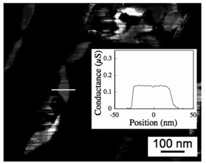
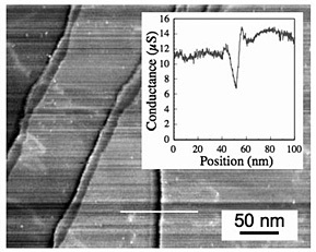
Figure 1 show an in-plane conductance image of graphene nano-islands. The coverage of graphene is carefully controlled by LEEM observation to make the graphene nano-islands. The conductance measurement reveals the islands consist of single- and double-layer graphene. The measurement with this nanotool enables us to measure electrical properties of nanostructures on insulative substrate without the need for fabrication processes including lithography. Figure 2 is an in-plane conductance image of double-layer graphene grown on SiC substrate. It was confirmed by LEEM that the domain size of the single-crystal double-layer graphene is larger than terrace width of SiC substrate and up to few micrometers. As shown in Fig. 2, the local conductance of graphene is strongly affected by the surface morphology of the SiC substrate. Notably, an atomic layer step buried under the graphene layer remarkably reduces the conductance of graphene. The conductance mapping with nanometer resolution will be helpful in developing carbon-based single-layer electronics.
This work was partly supported by KAKENHI (19310085, 20246064).
[1] H. Hibino et al., Phys. Rev. B 77 (2008) 075413.
[2] M. Nagase et al., Jpn. J. Appl. Phys. 46 (2007) 5639.
[3] M. Nagase et al., Nanotechnol. 19 (2008) 495701.
 |
 |
|||||
|
|