Materials Science Laboratory
Because of the excellent electrical performance of graphene, such as a
highest carrier mobility at room temperature, it is recognized as one of
the most promising candidates for the next-generation of electronics materials.
However, for its practical application, a remaining challenge is the formation
of graphene films with high quality and wafer-scale size to achieve compatibility
with a large-scale manufacturing process. To meet this challenge, we propose
a new approach for forming wafer-scale graphene, which is based on gas-source
molecular beam epitaxy (MBE). In this method, the substrate is not restricted
to specific ones as it is in other promising methods, such as graphene
formation by means of epitaxy on SiC [1] or on transition metals [2]. We
report here a demonstration of the gas-source MBE to show the feasibility
of our new approach for the formation of graphene [3].
In this experiment, about three atomic layers of graphene, prepared by
high-temperature annealing of 6H-SiC(0001) under an ultra-high vacuum,
were used as a substrate for the homoepitaxial growth. This substrate was
heated to 620ºC and cracked ethanol was supplied as a growth material.
After this growth, in situ x-ray photoelectron spectroscopy (XPS) measurements indicated that about
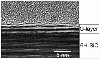
four monolayers of graphitic material were grown. The cross-sectional transmission
electron microscope image in Fig. 1 shows that this grown graphitic material
has a layered structure. These results show that graphene was grown. Meanwhile,
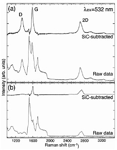
in the Raman spectra of the samples with and without the growth [Fig. 2],
we observed changes in the peak shape of the 2D-band and an increase in
the intensity of the G-band. This result supports the increase of graphene
thickness by the growth. However, a remarkable D-band peak was also observed
after the growth, indicating that the domain size of the graphene is small.
These results indicate that our new approach is feasible for the formation
of wafer-scale graphene and that it would be compatible with device fabrication
processes, although improvement in the crystal quality is needed.
[1] A. J. van Bommel, J. E. Crombeen, and A. van Tooren, Surf. Science
48 (1975) 463.
[2] L. C. Isett and J. M. Blakely, Surf. Science 58 (1976) 397.
[3] F. Maeda and H. Hibino, Phys. Status Solidi B 247 (2010) 916.
 |
 |
|||||
|
|