Optical Science Laboratory
Silicon (Si) is widely used to constitute electrical circuits, but it
is also a good material for constructing optical integrated circuits. Indeed,
optical waveguides and nanocavities have been fabricated on Si chips. However,
Si cannot be used to detect 1.5-µm light because it is transparent
in this wavelength region. Therefore, germanium (Ge) on Si detectors have
been fabricated, but these detectors exhibit a relatively large dark current
because of the 4 % lattice mismatch between Ge and Si [1]. In addition,
ion-implanted Si detectors have been studied, but they also suffer from
a large dark current because of the presence of defects [2]. If we can
fabricate an all-Si detector, we should benefit from a low dark current
because of the good crystal quality of Si. For this purpose, we need to
employ two-photon absorption (TPA) whose coefficient is usually very small.
In this study, we used a very high-Q photonic crystal (PhC) nanocavity to compensate for the low TPA coefficient
and to enable us to detect very weak optical light in an all-Si device
[3].
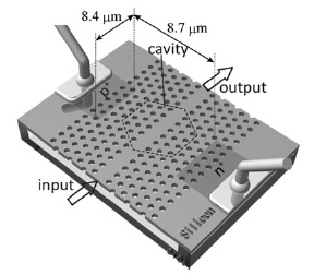
Figure 1 is an illustration of our pin integrated PhC nanocavity. The
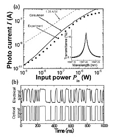
Q of the fabricated device was 4.3×10⁵ and the transmittance was 24 % [Fig. 2(a) inset]. The dark current was
just -15 pA when we applied a -3 V bias. Figure 2(a) shows photocurrent
versus input power. Due to the strong light confinement of the nanocavity,
the TPA current is visible at an extremely low input power of 10-8 W. The QE at an input power of 1.17 µW was very high at ~10 % (we define QE as 100 % when one photon generates one electron). This
value corresponds to 44 % of the cavity-coupled light being sufficiently
absorbed. Such a high detection efficiency with 1.55 µm light is
obtained because of the high Q of the PhC nanocavity.
We also demonstrated 0.1-Gb/s photo receiver operation using the same
device [Fig. 2(b)]. Only light that can resonate with the cavity was detected
electrically. This demonstration shows that our Si-chip integrated device
can be used for telecom light detection.
[1] S. Assefa, F. Xia, and Y. Vlasov, Nature 262 (2010) 80.
[2] M. Geis et al., Opt. Express 17 (2009) 5193.
[3] T. Tanabe et al., Appl. Phys. Lett. 96 (2010) 101103.
 |
 |
|||||
|
|