Distinguished Researchers

Akira Fujiwara was born in Tokyo, Japan on March 9, 1967. He received his B.S., M.S., and Ph.D. degrees in applied physics from The University of Tokyo, Japan in 1989, 1991, and 1994, respectively. In 1994, he joined NTT LSI Laboratories and moved to NTT Basic Research Laboratories in 1996. Since 1994, he has been engaged in research on silicon nanostructures and their application to single-electron devices. He was a guest researcher at the National Institute of Standards and Technology (NIST), Gaithersburg, MD, USA during 2003-2004. He received the SSDM Young Researcher Award in 1998, SSDM Paper Award in 1999, and Japanese Journal of Applied Physics (JJAP) Paper Awards in 2003 and 2006. He was awarded the Young Scientist Award from the Minister of MEXT (Ministry of Education, Culture, Sports, Science, and Technology) in 2006. He is a member of the Japan Society of Applied Physics and the IEEE.

Koji Muraki was born in Tokyo, Japan in 1965. He received his B.S., M.S., and Ph.D. degrees in applied physics from The University of Tokyo, Japan, in 1989, 1991, and 1994, respectively. In 1994, he joined NTT Basic Research Laboratories, Kanagawa, Japan. Since then, he has been engaged in the growth of high-mobility heterostructures and the study of highly correlated electronic states realized in such structures. He was a guest researcher at Max-Planck Institute, Stuttgart, Germany during 2001-2002. He is a member of the Physical Society of Japan and Japan Society of Applied Physics.
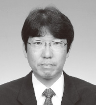
Hiroshi Yamaguchi was born in Osaka on October 30, 1961. He received the B.E., M.S. in physics and Ph.D. degrees in engineering from the Osaka University in 1984, 1986 and 1993, respectively. He joined NTT Basic Research Laboratories in 1986 and has engaged in the study of compound semiconductor surfaces using electron diffraction and scanning tunneling microscopy. His current interests are micro/nanomechanical devices using semiconductor heterostructures. He was a visiting research fellow in Imperial College, University of London, U.K. during 1995-1996 and a visiting research staff in Paul Drude Institute, Germany in 2003. He is a guest professor in Tohoku University from 2006 and a director of the Japanese Society of Applied Physics in 2008 and 2009. He is currently an executive manager of Physical Science Laboratory and a group leader of Nanostructure Technology Research Group. He is a member of the Japan Society of Applied Physics and the Physical Society of Japan.

Yoshitaka Taniyasu was born in Toyama, Japan on June 10, 1973. He received his B.E., M.E., and Dr. Eng. degrees in electrical engineering from Chiba University, Chiba, Japan in 1996, 1998, and 2001, respectively. He joined NTT Basic Research Laboratories in 2001. He has been engaged in wide bandgap semiconductor research. His current interests are epitaxial growth and device application of nitride semiconductors, especially aluminum nitride (AlN). He received the Young Scientist Award for the Presentation of the Excellent Paper at the Japan Society of Applied Physics (JSAP) in 2001, the Young Scientist Award at the Semiconducting and Insulating Materials Conference in 2007, and the Young Scientists’ Prize from the Minister of Education, Culture, Sports, Science and Technology in 2011. He is a member of the JSAP.

Norio Kumada was born in Gifu, Japan in 1975. He received his B.S., M.S., and Ph.D. degrees in physics from Tohoku University, Japan, in 1998, 2000, and 2003, respectively. In 2003, he joined NTT Basic Research Laboratories, Kanagawa, Japan. Since then, he has been engaged in the study of highly correlated electronic states realized in semiconductor heterostructures. He received Young Scientist Award of the Physical Society of Japan in 2008. He is a member of the Physical Society of Japan.