Physical Science Laboratory
The electronic states of phosphorous atoms in silicon (Si) are now attracting
much attention because they could be useful for solid-state quantum computers.
We report a strong Stark effect in electroluminescence (EL) from phosphorous-doped
silicon-on-insulator (SOI)-MOSFETs when electrons are injected into the
sub-10-nm-thick SOI channel by tunneling [1].
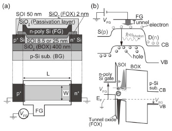
The devices were SOI-MOSFETs with an n-type polycrystalline Si (poly-Si)
tunneling gate [Fig. 1(a)]. Two SOI thicknesses (tSOI) of 8.5 and 25 nm were prepared. The thicknesses of the front-gate oxide
(FOX), and the buried oxide (BOX) were approximately 2 and 400 nm, respectively.
The potential profiles for the device are shown in Fig. 1(b). Due to the
thermal treatment for the device fabrication, the SOI channel was phosphorous-doped
on the order of 1017 cm-3. Electroluminescence spectra were taken at temperature (T ) of 80 K. Electrons are injected from the front gate into the SOI channel,
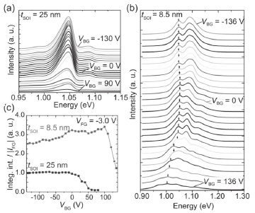
while holes are injected from the boron doped p+ contact. Figure 2(a) shows the VBG dependence of the EL spectrum for the device with tSOI of 25 nm. The EL intensity decreased as VBG was positively increased, producing an electric field in the SOI so that
electrons distribute near BOX/SOI interface. Then electrons and holes are
strongly separated, which results in the decrease of the EL intensity.
On the other hand, the VBG dependence of the EL spectra for tSOI of 8.5 nm showed complicated behavior [Fig. 2(b)]. The peak for a neutralized donor and free-hole recombination (D0-h) showed Stark shift of up to 50 meV at VBG of 136 V. The EL intensity kept a higher value even when that for 25 nm became almost zero, and then suddenly decreased around VBG of 80 V [Fig. 2(c)]. The sudden change of the EL intensity can be explained
by electron dissociation from strongly bound states. In contrast to the
thicker QW, the ground state of triangular well at the BOX interface in
the QW for tSOI of 8.5 nm is higher than that of phosphorous-bound state at low electric
field. Therefore, electrons bound at phosphorous atoms hardly dissociate
in the thin QW. This is the reason for the difference in the specific field
needed to cause the sudden decrease of the EL intensity.
[1] J. Noborisaka et al., Appl. Phys. Lett. 98 (2011) 033503.
 |
 |
|||||
|
|