Physical Science Laboratory
Single-electron (SE) transfer is expected to be used in ultralow power
consumption circuits and current standards in metrology. Accuracy of the
SE transfer is crucial for determining bit errors or uncertainty in the
current standards. A sufficiently low error rate, typically an error per
transferred electron of about 1 part in 108, is necessary for the current standards. Here we demonstrate an absolute
accuracy evaluation of the SE transfer [1] in high-speed transfer devices
constructed by using Si nanowire metal-oxide-semiconductor field-effect
transistors (MOSFETs) [2].
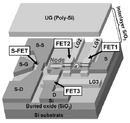
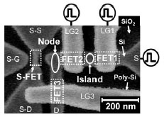
Figures 1 and 2 show a schematic diagram and a scanning electron microscope
image of the device, respectively. The SE transfer device comprises three
Si nanowire MOSFETs (FET1, 2, and 3) on a silicon-on-insulator wafer. A
high-sensitivity charge sensor is composed of another Si nanowire MOSFET
(S-FET). For the absolute evaluation of accuracy of the SE transfer, a
node is first formed by turning FET3 off. Then, pulse voltages are applied
to FET1, FET2, and the source (S) to shuttle an SE between the source and
the node. Finally, we evaluate the transfer error by detecting the number
of electrons in the node during the SE shuttle transfer. The merit of this
scheme is that the error of the high-speed transfer is evaluated by detecting
the average number of electrons in the node with a low-speed sensor. As
a first step, we carried out single-shot measurement and thereby separated
SE captures into the node and SE ejections from the node to investigate
the transfer mechanism.
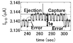
Figure 3 shows a typical result of the detection during the SE shuttle transfer at a temperature of 17 K. The abrupt changes of the detection current (IS-D) indicate the capture and ejection of an SE. Here, two capture errors are observed. From longer measurements, the best error rates of the capture and ejection are estimated to be about 2.1 % and 0.25 %, respectively. The former can be explained by thermal fluctuations, indicating the possibility of achieving high-accuracy transfer by reducing temperature or scaling down the device size. The latter can not be explained by thermal fluctuations. From the dependence of the pulse voltage amplitude, we attribute it to transfer mediated by a trap level. Since the trap-mediated transfer shows low error, it could be possible to achieve high-accuracy SE transfer.
[1] G. Yamahata et al., Appl. Phys. Lett. 98 (2011) 222104.
[2] A. Fujiwara et al., Appl. Phys. Lett. 92 (2008) 042102.
 |
 |
 |
||||||||
|
|
|