Accuracy Evaluation of Si Single-Electron Transfer Devices at Extremely Low Temperature
Gento Yamahata, Katsuhiko Nishiguchi, and Akira Fujiwara
Physical Science Laboratory
One electron can be accurately manipulated by means of single-electron (SE) transfer. This technique can be applied to ultralow-power-consumption devices and current standards in metrology. For these applications, a transfer error rate of below 10-8 is necessary. Although we have reported an absolute accuracy evaluation of Si SE transfer devices, the transfer error rate has been about 10–2 due to thermal fluctuation at T = 17 K [1]. Here we report an absolute accuracy evaluation at T = 30 mK, where the error rate is about 10–4. In addition, we theoretically show that the error rate can be reduced to a value on the order of 10–8 [2].
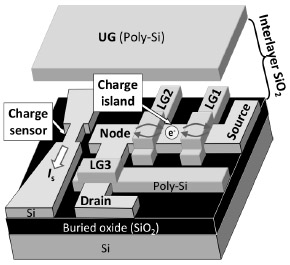
Figure 1 shows a schematic of the device. On an Si-on-insulator substrate, we fabricated an SE transfer device, which comprises three nanowire transistors (LG1, LG2, and LG3 are gate electrodes), and a charge sensor, which comprises a nanowire transistor (UG is gate electrode). When we apply a positive voltage to LG3 and pulse voltages to LG1 and LG2, a transfer current via a charge island between LG1 and LG2 is generated between the source and drain. In addition, when a node is formed by applying a negative voltage to LG3, an SE is shuttled by applying one more pulse voltage to the source. During the shuttle SE transfer, we detected changes in the number of electrons in the node by measuring current Is passing through the charge sensor to evaluate the transfer errors.
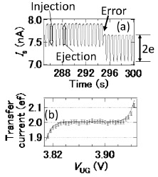
In the experiment, we evaluated the transfer error during the transfer of two SEs. Figure 2(a) shows changes in Is during the shuttle transfer of two SEs, where the abrupt increase and decrease in Is correspond to the ejection and injection of the two SEs, respectively. In this measurement, we observed one error. By counting the number of such errors, we obtained the error rate of about 10–4, which is two orders magnitude better than the previous result. The error originates from an effective device-temperature (Teff) increase caused by the pulse voltage. In addition, we estimated the lower bound of the error rate from a theoretical fit to the transfer current (Fig. 2(b)). When Teff was decreased by decreasing the amplitude of the pulse voltage, the transfer mechanism changed and the lower bound of the error rate decreased. At minimum Teff (~ 5 K), the lower bound of the error rate is on the order of 10–8.
This work was partly supported by the Funding Program for Next Generation World-Leading Researchers of JSPS.
- [1]
- G. Yamahata, K. Nishiguchi, and A. Fujiwara, Appl. Phys. Lett. 98 (2011) 222104.
- [2]
- G. Yamahata, K. Nishiguchi, and A. Fujiwara, Phys. Rev. B 89 (2014) 165302.
 |
 |
- Fig. 1.
- Schematic of the device.
|
|
- Fig. 2.
- (a) Typical result of counting the number of SEs. (b) Typical transfer current (circles) and fit (line).
|
<< Prev | Contents | Next >>