Encapsulated Gate-All-Around InAs Nanowire Field-Effect Transistors
Semiconductor nanowires (NWs) are attracting growing interest as promising building blocks for the next generation of nanoelectronic devices. InAs NWs are of particular importance in view of application to high-speed, low-power-consumption field-effect transistors (FETs) due to their high intrinsic electron mobility. We fabricated InAs NW FETs with a gate-all-around (GAA) structure, which enables improved electrostatic control, by employing a novel two-step gate electrode formation method. The gate electrode overlaps the source/drain electrodes, leading to a dramatic increase in driving current as a result of reduced series resistance [1].
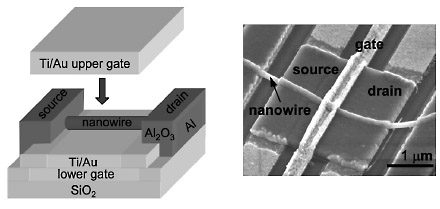
InAs NWs are grown via the Au-catalyzed vapor-liquid-solid (VLS) mode in a MOVPE system. The as-grown NWs are conformally coated with 6 nm of Al2O3, used as high-k gate dielectric, via atomic layer deposition (ALD). The NWs are then transferred to another Si/SiO2 substrate with a prepatterned Ti/Au lower gate electrode (Fig. 1). Source and drain Ohmic contact regions are defined by electron-beam lithography at both ends of the NW, followed by Ar plasma etching to remove the surface oxides, and deposition of Al without breaking vacuum. This way, Ohmic contacts with low resistance are obtained. The Al surface is then oxidized to form an Al2O3 insulator in order to ensure electrical isolation between the upper gate and the source/drain electrodes. Finally, the Ti/Au upper gate is deposited overlapping the source/drain electrodes, thus encapsulating the NW and realizing GAA structure.
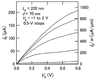
Figure 2 shows drain current Id vs. drain voltage Vd characteristics for various gate voltages Vg, for a FET device with gate length Lg = 220 nm and NW diameter d = 70 nm. The device exhibits n-type FET operation with a threshold voltage of 0.39 V. Drain current normalized by the NW circumference, w = πd, is also shown. Normalized transconductance, gm/w, is 0.55 S/mm at Vd = 0.5 V, which outperforms existing FETs with homogeneous InAs NW channels. These superb on-state properties are ascribed to improved electrostatic control by GAA structure and to the reduction in series resistance by the gate-overlap geometry.
- [1]
- S. Sasaki,G. Zhang, K. Tateno, H. Suominen, Y. Harada,S. Saito,A. Fujiwara, T. Sogawa, and K. Muraki, Appl. Phys. Lett. 103 (2013) 213502.
 |
 |
|
|