Optical Nanocavity Formed by a Semiconductor Nanowire and a Si Photonic Crystal
Semiconductor nanowires are attractive for their small diameters of less than 100 nm. In particular, III-V semiconductor nanowires can be used in a variety of structures, such as core-shell and multilayer heterostructures and p-i-n junctions, by arranging growth sequences in epitaxial growth, which may enable us to realize small optical devices with low energy consumption. However, a nanowire itself can not provide sufficient optical confinement to achieve the desired device performance because it is too small to match the wavelength of light. On the other hand, Si photonic crystal provides optical confinement with the dimension of the wavelength of light; however, it requires a regrowth process in order to incorporate optically active material. Therefore, the types of materials we can use with Si photonic crystal are limited.
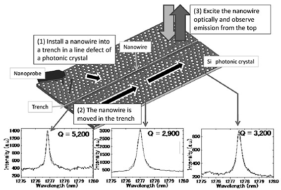
Here, we demonstrate that a nanocavity can be created in a photonic crystal by placing a nanowire in a trench in a line defect of Si photonic crystal. We move the nanowire by means of AFM manipulation, in which a nanoprobe can be used to drag a small object. In addition, the position of the nanocavity can be shifted by moving the nanowire in the trench (Fig. 1) [1]. The nanocavity is a mode-gap cavity generated by partially changing the effective refractive index in the line defect [2, 3]. We obtained the highest Q-factor of 9500 (resonant wavelength: 1.5 µm) for a sample with a InAsP/InP heterostructure nanowire (2620-nm length, 85-nm diameter) installed into a trench in a line defect (lattice constant of 416 nm, trench width of 150 nm, depth of 75 nm) of a photonic crystal. As the the Q-factor for the movable cavity can vary at each nanowire position, we can evaluate the Q-factor dependence of cavity photon lifetime by evaluating each photon lifetime in the nanowire-induced cavities with an identical nanowire placed at different positions. We confirmed that the photon lifetime decreases with increasing Q-factor, which can be attributed to the Purcell effect. We obtained a photon lifetime of 91 ps for a nanowire-induced photonic crystal cavity with a Q-factor of 5200, which is the shortest lifetime ever achieved for a III-V semiconductor nanowire.
This demonstration indicates the possibility of realizing photonic integrated circuits on demand, where optically active material is installed into a universal photonic crystal substrate to provide a nanocavity with the desired functionality.
- [1]
- M. D. Birowosuto, A. Yokoo, G. Zhang, K. Tateno, E. Kuramochi, H. Taniyama, M. Takiguchi, and M. Notomi, Nature Mater. 13 (2014) 279.
- [2]
- M. Notomi and H. Taniyama, Optics Express 16 (2008) 18657.
- [3]
- M. D. Birowosuto, A. Yokoo, H. Taniyama, E. Kuramochi, M. Takiguchi, and M. Notomi, J. Appl. Phys. 112 (2012) 113106.
|
|
|
|