Transition metal dichalcogenides (TX2) belong to a family of two-dimensional layered materials, where adjacent layers are weakly bound by van der Waals forces, like in graphite. These materials offer a large variety of properties, from insulating/semiconducting to metallic ones, depending on the combination of T and X. Among them, we have been focusing on semiconducting MoSe2.
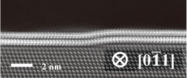
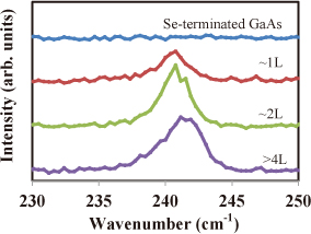
We grew wafer-scale MoSe2 thin films on Se terminated GaAs(111)B substrates using the molecular beam epitaxy (MBE) method. The Scanning transmission electron microscope (STEM) image in Fig. 1 shows that two-monolayer (2L)-thick MoSe2 is grown in a layer-by-layer manner. It also indicates that the MoSe2 layers can climb over the monolayer step of GaAs. Though Fig. 1 shows an STEM image for a double-layer MoSe2, it should be noted that the layer number can be varied with growth time. We carried out Raman spectroscopy measurements and investigated layer number dependence. Figure 2 shows Raman spectra around the A1g peak for single-layer (1L), double-layer (2L), and more-than-four-layer (> 4L) MoSe2 thin films. The spectrum for Se-terminated GaAs is also shown as a reference. According to a previous report on MoSe2 mechanically cleaved from bulk crystal [1], the A1g peak shifts to a higher wavenumber with an increasing number of layers because of multiple interlayer interactions. The A1g peaks in our MoSe2 thin films also show the blue shift (Fig. 2) when the layer number increases. The layer number of our films estimated from the positions of A1g peaks, using reported values for cleaved samples as references [1], well coincides with that directly determined by STEM observation. On the other hand, splitting of the A1g peak is not clearly observed in our film samples, which is in contrast to the cleaved ones with thicknesses of > 3L [1]. The peak splitting originates from the minute difference in vibration frequencies between the in-phase and out-of-phase vibrations and is very sensitive to the layer number [1]. Therefore, the absence of the peak splitting in our films likely stems from a fluctuation of the layer number (±1 layer) due to partial formation of growth nuclei on atomically flat surfaces.
Our results indicate that wafer-scale MoSe2 thin films with a controlled layer number can be prepared by MBE, which is widely used for growth of high-quality thin films of conventional semiconductors. Application of this technique to other TX2 materials may allow fabrication of heterostructures consisting of various TX2 materials.