Optical memory is a key device for all-optical routing/signal-processing. The former is applicable for both broadband networks in telecommunication and data centers and on/off-chip optical interconnects for large-scale CMOS electronic chips. The transportation of photonics over electronics is considered to be a way of dealing with the huge data-transfer cost (power, heat, space, overhead), which becomes serious as the integration density increases. We have previously demonstrated an ultra-small optical random access memory (o-RAM) with an ultra-small operating power (30 nW) by using a high-Q photonic crystal nanocavity [1]. However, the highly dense integration of many o-RAMs is difficult to achieve with the previous nanocavity design.
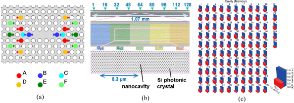
In this study, we employed a novel three-missing-hole nanocavity (L3) with the systematic tuning of multiple holes [Fig. 1(a)], which enhanced the Q factor 10-fold compared with the conventional L3 [2]. Thanks to the narrow cavity mode linewidth, enhanced carrier-plasma bistability, and wide free spectrum range, we could employ wavelength-division-multiplexing technology to realize write/read-out access to every o-RAM via one common side-coupling waveguide, and eventually 128-bit o-RAMs were integrated as a simple tandem array of 128 L3s [Fig. 1(b)] [3]. The lattice constant a at every L3 was changed from 408 to 424 nm in 0.125 nm steps to set a wavelength spacing of ~30 GHz and the cavity spacing was 20a. The total length of the 128-bit integrated o-RAM was only 1.1 mm. We fabricated this precise 128 L3 array in a Si photonic crystal using electron beam lithography. In the experiment, we realized o-RAM operation by injecting bias light at the wavelength of the target o-RAM, and we switched the “1” state and “0” state with set/reset pulses. As shown in Fig. 1(c), we successfully demonstrated the o-RAM operation of 105 L3s. In addition to the groundbreaking jump in bit number from the several bits of conventional o-RAMs, the total operating power of 30 mW was surprisingly low. We applied the same technology to a more sophisticated InP-based nanocavity with an embedded buried heterostructure and realized multi-bit o-RAM operation on lower power consumption and a second time scale [3].
The success of state-of-the-art nanophotonics has opened the way to the monolithic integration of 1000 nanophotonics devices (or 1000 bits) and even one million devices on a chip by employing parallel integration.