Recent CMOS processors employ multi-core architectures, and the network of interconnections between cores is very important. However, there is a bandwidth bottleneck in current electrical interconnects. To overcome it, many researchers are attempting to form optical interconnects on CMOS chips because they provide a larger bandwidth with lower energy consumption. We have studied lambda-scale embedded active-region photonic-crystal (LEAP) lasers on InP substrates as light sources for on-CMOS-chip optical interconnects [2]. Here we report the continuous-wave (CW) operation of LEAP lasers on Si substrates as the first step to realizing on-CMOS-chip light sources.
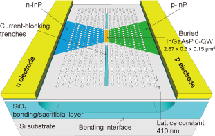
Device fabrication procedures were similar to those we have reported elsewhere [3]. We carried out crystal (re)growths and lateral p-i-n junction formation on InP substrates to form an ultrasmall buried heterostructure (BH). After SiO2 had been deposited on the InP substrates, the surfaces were planarized by chemical mechanical polishing (CMP) and the 2-inch InP substrates were bonded to 2-inch Si substrates. After the bonding, the host InP substrates were removed by mechanical polishing and wet etching so that a 250-nm-thick III-V membrane was transferred onto the Si. Two-dimensional photonic-crystal (PhC) holes were then formed by electron-beam lithography and dry etching, followed by metallization processes. Figure 1 shows a schematic of the fabricated device.
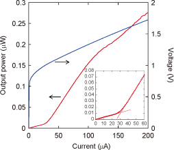
We injected current and measured light output from the direction normal to the wafer at room temperature. The measured output power and applied voltage versus injected current (L-I-V characteristics) are shown in Fig. 2. We achieved a CW operation of the LEAP lasers on Si substrates with a threshold current of 31 μA, which is the record low value among semiconductor lasers on Si. The device showed single-mode operation with a lasing wavelength of 1501 nm. This achievement reveals that the LEAP lasers can operate not only on InP but also on Si substrates, and we believe this is an important step to realizing LEAP lasers as on-CMOS-chip light sources.