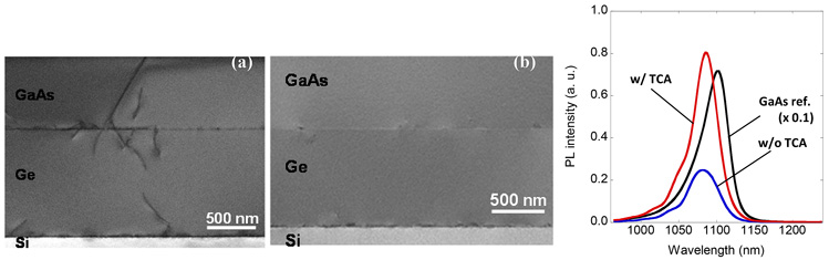
Dislocation Reduction in MOVPE-grown GaAs/Ge Layers onSi Substrates by Thermal Cycle Annealing
Direct growth of III-V compound semiconductor has been desired for 30 years. Recently, incorporating a Ge buffer layer between Si and GaAs III-V compound semiconductor has been studied to improve the crystalline quality because Ge’s lattice constant is very close to GaAs’s [1]. Monogermane (GeH4) is widely used as a material source for the Ge buffer layer. However, GeH4 is explosive material. Thus, the Ge buffer layer cannot be grown in the same reactor used for GaAs epitaxial growth [2]. Instead of using GeH4, we used metal-organic material iso-butyl germane (IBGe) as a Ge precursor. The Ge buffer layer and GaAs were grown in the same metal-organic vapor phase epitaxy (MOVPE) reactor. Figure 1(a) shows the cross-sectional transmission electron microscopy (TEM) image of a GaAs/Ge structure grown on Si substrate. At the boundary between the GaAs and Ge layer, dislocations can be seen. The dislocations penetrated the epitaxial layer surface. To reduce the dislocations, we performed thermal cycle annealing (TCA) after the GaAs and Ge layer growth [3]. As shown in Fig. 1(b), the dislocations at the GaAs/Ge boundary were significantly suppressed by TCA. Moreover, by employing TCA, the intensity of photoluminescence (PL) measured from InGaAs/GaAs multiple quantum wells (MQWs) grown on the GaAs epitaxial layer increased by a factor of three (Fig. 2). This is indicates that the crystalline quality was improved by TCA. On the other hand, the PL intensity was 11% smaller than that for MQWs on GaAs substrate. Further improvement of growth and annealing conditions will provide crystalline quality comparable to GaAs substrate. These results indicate that the MOVPE-grown GaAs/Ge layers are well-suited for integrating a light source onto Si substrate.
- [1] A. Lee et al., Opt. Express 20, 22181 (2012).
- [2] M. E. Groenert et al., J. Appl. Phys. 93, 362 (2003).
- [3] R. Nakao et al., in Electronic Materials Symposium 34, Th-2-3 (2015).
|
|
| Fig. 1. Cross-sectional TEM images of (a) as-grown GaAs/Ge structure on Si substrate and (b) after TCA. | Fig. 2. PL spectra from MQWs. |