Demonstration of Efficient Mode Conversion for Deep-subwavelength Plasmonic Waveguides
Plasmonic waveguides enable us to utilize light-propagating modes much smaller than a wavelength dimension in photonic integrated circuits. In particular, nanomaterials such as nanowires and two-dimensional (2D) materials interact efficiently with light in deep-subwavelength plasmonic waveguides, and their combination may lead to ultracompact, ultrahigh-speed photonic devices. On the other hand, plasmonic waveguides have a large propagation loss, and thus conventional low-loss dielectric waveguides are needed for long distance propagation. However, it is difficult to efficiently connect two waveguide modes that have fundamentally different sizes and characteristics. Thus, the waveguide thickness was almost unchanged in previously reported mode converters. In this study, we demonstrate highly efficient (–1.7 dB) mode conversion between a Si-wire waveguide (400 × 200 nm2 core
size) and a plasmonic waveguide with a metal-insulator-metal (MIM) structure (50 × 20 nm2 core size) [1]. The waveguide thickness was reduced from 200 nm to 20 nm, resulting in a large reduction in core size. In addition, the core size of the connected MIM waveguide decreased to (λ/n)2/2000 (λ = wavelength, n = reflective index).
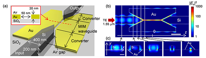
Our converter consists of a 2D laterally tapered structure, and there is a small gap between the Si and the metal [Fig. 1(a)]. Figures 1(b) and (c) show the calculated field profile at a wavelength of 1.55 μm. The eigenmode of the Si-wire waveguide has side lobes, which are attracted to the air gap and are adiabatically connected to the MIM mode. Investigating the structural parameter dependence of the coupling efficiency, we found that the coupling efficiency is greatly increased both by optimizing the taper length and by introducing the small air gap. This enables highly efficient, full three-dimensional (3D) mode conversion, where the mode size is squeezed laterally and vertically, without the need to introduce a 3D tapered structure accompanied by a complicated fabrication process. We measured the fabricated samples and estimated the coupling efficiency. The experimentally obtained coupling efficiency was very high and –1.7 dB for an air gap width of 40 nm and a taper length of 600 nm. This efficiency value was consistent with the calculated result (–1.4 dB). We believe that our mode converter will provide a new deep-subwavelength photonic platform.
This work was supported by JSPS KAKENHI JP15H05735.
- [1] M. Ono et al., Optica 3, 999 (2016).
|
| Fig. 1. (a) Schematic structure of the mode converter. (b) Cross-sectional top view of the calculated field profile for an air gap width of 40 nm and a taper length of 400 nm at y = 10 nm. Scale bar, 500 nm. (b) Cross-sectional side views of the calculated field profile. Scale bar, 200 nm. |