Efficient Light-to-voltage Conversion by Ultralow-capacitanceNano-photodetector
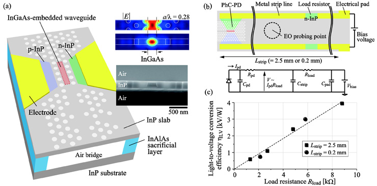
Photodetectors (PDs) to use as a receiver in a dense on-chip photonic processor requires low-energy consumption and small size. However, the energy consumption of a conventional photoreceiver is dominated by the electric amplifiers connected to the PD. An ultralow-capacitance PD can overcome this limitation, because it can generate large voltage without an amplifier when connected with a high-impedance load. By our fabrication technique of the buried heterostructure to embed the compact InGaAs absorber in the photonic crystal (PhC) waveguide [Fig. 1(a)] [1], we demonstrated the ultrasmall PD with a length of 1.7 μm and a theoretical capacitance of only 0.6 fF. Such a short PD still showed the optical responsivity as high as 1 A/W and the fast response with a bit rate of 40 Gbit/s. A resistor-loaded PD was also fabricated to evaluate the light-to-voltage conversion [Fig. 1(b)]. We utilized an electro-optic probing method to measure the voltage across the strip lines, which is generated from the photocurrent and the load resistor. As a result, we obtained a light-to-voltage conversion efficiency of 4 kV/W [Fig. 1(c)], which is actually as large as conventional receivers integrated with amplifiers. Although the operation bandwidth was limited by the parasitic capacitance of the strip lines that were required in the EO probe measurement, a 40 Gbit/s operation will be expected if we only take the ultrasmall PD capacitance into account. These results offer the realization of an ultralow-energy amplifier-less receiver by using an ultrasmall-capacitance PD, and therefore are step toward a densely-integrated photonic network/processor on a chip.
This work was partly supported by CREST (JPMJCR15N4), JST.
- [1] K. Nozaki et al., Optica 3, 483 (2016).
|
| Fig. 1. (a) Photonic crystal PD. Insets show the optical field distribution (upper) and the cross-sectional photograph (lower). (b) Resistor-loaded PD and its equivalent circuit. (c) Light-to-voltage conversion efficiency vs load resistance characteristic. |