Visualizing the Photonic Band Structure
Masaya Notomi and Toshiaki Tamamura
Materials Science Laboratory
Since it had been predicted that photonic insulators can be developed by
photonic crystals possessing full bandgap, many researchers have been trying to
realize them with expectations that they would enable us to realize ultra-small
optical circuits and to artificially control spontaneous emission. However, a
well-known fact that light likes to go straight leads to essential difficulty in
realizing 3D photonic insulators. One of problems in the photonic crystal
research is that we cannot experimentally measure the photonic band structure.
We noted on the fact that beam propagation in photonic crystals is governed by
their band structure, and clarified that it is possible to construct the band
structure from the beam propagation measurement. Furthermore, we succeeded in
direct measurement on the band structure of a 3D Si/SiO2 photonic crystal which
was fabricated by autocloning mode of bias-sputtering on a lithographically
patterned substrate (in collaboration with Tohoku University).
Beam propagation direction of Bloch waves in photonic crystals is a normal
direction of equi-frequency surface of the photonic band, which corresponds to
Fermi surface in metals. Therefore, we can deduce the shape of equi-frequency
surface from the information on wavevectors of incident waves, beam propagation
angles, and symmetry of crystal, and we can determine the band structure by
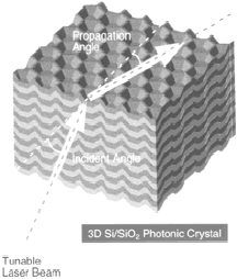
sweeping the wavelength. We launched a nearly-collimated beam to the cleaved
edge of the 3D photonic crystal sample, and determined the propagation direction
by CCD camera monitoring (Fig. 1). Figure 2 shows the photonic band structure
around the K point determined by the measured data of propagation angles. This
figure shows that a gap is open on the K point around a wavelength of 0.93 μm,
and two bands having three-hold rotational symmetry are formed around this
photonic gap.
The method described here is considerably simple and accurate, and it enables us
to determine the detailed shape of equi-frequency surface which is essentially
important to design the photonic crystal circuit. In addition, such detailed
band information is quite important on currently-going research works toward 3D
full photonic bandgap materials.
Fig. 1: Schematic of a 3D Si/SiO2 photonic crystal and set up for the band structure determination experiment.
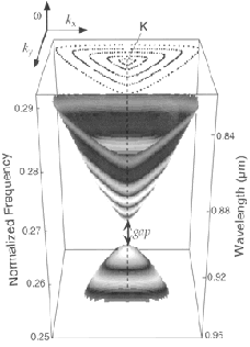
Fig. 2: Experimentally determined 3D photonic band structure (w-kx-ky) around the K of the Si/SiO2 photonic crystal.