 (a)
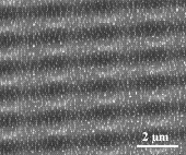
after deposition at 400°C
(a)
after deposition at 400°CPrecise Control of Island Formation Using Atomic Step Band Networks
Yoshikazu Homma, Paul Finnie, and Toshio Ogino
Device Physics Laboratory
For the fabrication of quantum effect semiconductor devices, it is essential to obtain good control of the size and position of nanometer-scale structures. So far, self-assembling of 3D islanding due to strain on lattice mismatched substrates has been intensively studied. However, it is difficult in this method to avoid uncertainty in the size and position of islands. On the other hand, nano-fabrication using scanning probe methods has high structural controllability but lacks throughput. We are developing a novel nano-fabrication technique, which arranges atomic steps on the wafer scale and uses these steps as templates. We have already shown that wire structure growth along the step bands is possible by using selectivity of nucleation between terraces and step bands. Here, we further extend this technique to selectively form liquid metal islands in a self-assembling manner.
Figure 1 shows the alignment of Au islands using regularly arranged step bands on Si(111). The regular step band network was obtained by annealing a patterned substrate with a small hole array which had been formed lithographically. Deposition of Au at 400°C on to the substrate creates a high density of liquid Au-Si islands as shown in (a). Annealing at 560°C leads to coalescence and annihilation of islands through attachment and detachment of Au atoms from islands. Finally the islands remain at energetically stable positions as shown in (b). By adjusting the annealing temperature, the diffusion length of surface atoms is tuned to the pattern period, resulting in only one island every pattern unit. The island size is precisely controllable depending on the pattern period and the amount of deposition. Similar island alignment was obtained for Ga. We have also demonstrated that Si pillars can be grown selectively at such Au island positions by chemical-vapor deposition.
[1] T. Ogino, H. Hibino, and Y. Homma, Jpn. J. Appl. Phys. 34(1995) L668.
[2] P. Finnie and Y. Homma, Appl. Phys. Lett. 72(1998) 827.
[3] Y. Homma, P. Finnie, and T. Ogino, Appl. Phys. Lett. 74(1999) 815.
(a)
after deposition at 400°C
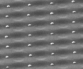 (b) after annealing at 560°C
Fig. 1: SEM images of Au islands on Si(111) with arranged step structures.