Distinguished Technical Member
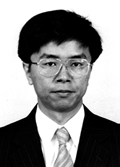
Naoki Kobayashi was born in Osaka on January 16, 1953. He received the B.S., M.S., and Ph.D. degrees in applied chemistry from the Osaka University of in 1975, 1978, and 1985, respectively. He joined NTT Basic Research Laboratories in 1978. He was a guest scientist of CNET Bagneux Laboratory, France, in 1987 and a guest scientist of the Prof. Stringfellow's laboratory in the University of Utah in 1993. Since 1978 he has engaged in the study of liquid phase epitaxy of compound semiconductors and its application to semiconductor lasers, the development of flow-rate modulation epitaxy and the growth of atomic-layer structure, and in-situ optical monitoring of the surface during MOVPE growth. His current interest is the in-situ control of MOVPE growth of group III-nitrides. He is an editor of the Japan Society of Applied Physics, and a member of the Physical Society of Japan, the Japan Society of Applied Physics, and the Surface Science Society of Japan.
Yoshikazu Homma was born in Niigata on April 11, 1953. He received the B.E. and M.S. degrees in physics from Tohoku University in 1976 and 1978, respectively. He joined NTT Laboratories in 1978, where he received his Ph.D. degree in applied physics from the University of Tokyo in 1987. He was a guest scientist in Gesellshaft fur Strahlen-und Umweltforschung, Munich, Germany during 1987-1988. Since 1978 he has engaged in researches of ultratrace analysis of semiconductors using secondary ion mass spectrometry, in-situ imaging of growing surfaces using ultrahigh vacuum scanning electron microscopy, and atomic step engineering on semiconductor surfaces. His current interest are the development of in-situ surface microscopy with atomic resolution and nanostructure fabrication. He is an editor of Journal of the Japan Society of Analytical Chemistry, and Journal of the Mass Spectrometry Society of Japan, and a member of the Physical Society of Japan, the Japan Society of the Applied Physics, the Surface Science Society of Japan, the Japan Society for Analytical Chemistry, and the Mass Spectrometry Society of Japan.
Yoshiro Hirayama was born in Kanagawa on July 18, 1955. He received the B.E., M.S. and Ph.D. degrees in electrical engineering from the University of Tokyo in 1978, 1980 and 1983, respectively. He joined NTT Basic Research Laboratories in 1983. He was a guest scientist in Max-Planck-Institut fur Festkorperforschung, Stuttgart, Germany during 1990 - 1991. Since 1983 he has engaged in the study of semiconductor nano structures fabricated by focused-ion-beam technique, transport characteristics of semiconductor mesoscopic systems and ballistic transport in high-mobility semiconductors. His current interests are transport properties of semiconductor layer and nano structures including carrier interaction phenomena. He is a research coordinator of NEDO international joint research project (NTDP-98) since 1998 and also a coordinator of CREST research team for interacting carrier electronics since 1999. He is an editor of Japanese Journal of Applied Physics, and a member of the Japan Society of Applied Physics, the Physical Society of Japan and IEEE.