Yukinori Ono, Yasuo Takahashi, and Katsumi Murase
Device Physics Laboratory
The single-electron transistor (SET) is a promising element for future extremely-large-scale integrated circuits because of its small size and ultralow power consumption. However, very few experiments have addressed the integration of SETs because their fabrication is difficult even when state-of-the-art nanolithography is used. We have therefore developed a method of fabricating integrated-circuit-oriented SETs, which we call Vertical Pattern-Dependent Oxidation (V-PADOX) [1], and have applied it to the fabrication of a directional current switching device. Very recently, we have successfully fabricated an inverter, the most elemental circuit for logic LSIs, using V-PADOX and observed its operation [2].
In V-PADOX, we first form a fine trench on a thin Si layer of a silicon-on-insulator wafer and successively make a specific pattern by etching the Si with the trench. Then, V-PADOX applies thermal oxidation to the pattern, which enables the automatic formation of two SETs at the same time. The resultant SETs have a high voltage gain even at a high temperature of 30 K. This is important in constructing logic LSIs and has never been achieved by the former SETs. Furthermore, by changing the shape of the patterned silicon, V-PADOX allows us to make various types of circuit configurations, such as parallel and cascaded connections of SETs. Figure 1 shows an atomic force microscope (AFM) image of the inverter circuit that enjoys the above merits of the method. Two SETs are packed in a tiny area; 100 x 100 nm2 for each SET. Figure 2 shows the input-output transfer characteristic of the inverter. The output voltage exhibits a full logic swing for a power supply voltage (VDD) of 20 mV. In addition, the voltage gain (the dotted line) exceeds unity, which guarantees signal transfer to any following gates. The present result is the first experimental demonstration that single-electron logic circuits can be constructed based on CMOS logic.
[1] Y. Ono et al., IEEE Trans. Electron Devices 47 (2000) 147.
[2] Y. Ono et al., Appl. Phys. Lett. 76 (2000) 3121.
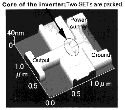
Fig. 1. AFM image of the inverter. The input terminal (not shown) is placed over the SETs.
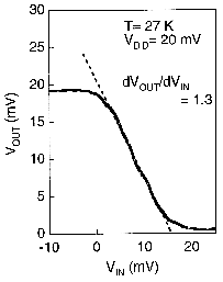
Fig. 2. Input-output transfer characteristic.
Back