Å@
Atsushi Nishikawa, Kazuhide Kumakura, and Toshiki Makimoto
Materials Science Laboratory
Å@
Å@Due to wide band gap and high critical electric field of GaN, GaN-based
electronic devices are promising for high-power and high-temperature operation.
Although a lateral conducting structure using a semi-insulating substrate
such as sapphire is usually fabricated for GaN-based devices, a vertical
conducting structure using a conductive substrate is advantageous for lower-loss
and higher current density. Therefore, GaN-based vertical conducting devices
are expected to be preferable for high-power electronic device applications.
So far, the study on GaN-based vertical pn junction diode was insufficient
because of a high-resistance p-GaN layer and a buffer layer to grow a GaN
layer on a hetero-substrate. We have overcome these difficulties by using
an InGaN layer for the p-type layer and GaN substrate on which a GaN layer
can be directly grown. The diode fabricated in this study exhibits a high
breakdown voltage with a low on-state resistance [1].
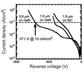
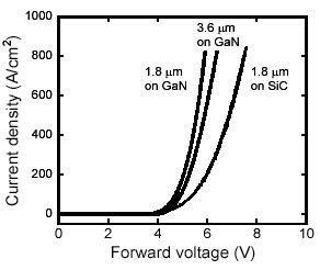
Å@The samples were grown on n-GaN substrates, using metalorganic vapor
phase epitaxy (MOVPE). The sample structure consists of a 1.8-mm or 3.6-mm-thick lightly doped n-GaN layer and a 140-nm-thick p-InGaN layer.
For comparison, the same diode structure with 1.8-mm-thick n-GaN was grown on
a conductive SiC substrate. Figure 1 shows reverse current-voltage (I-V) characteristics. The leakage current of the diode on a GaN substrate
is one order of magnitude lower than that on a SiC substrate due to the
better crystal quality of GaN grown on a GaN substrate. Since a thick crack-free
GaN layer can be grown on a GaN substrate, the breakdown voltage increases
with increasing n-GaN layer thickness. For the 3.6-mm-thick GaN
layer, the breakdown voltage (VB) reaches as high as 571 V. At the
same time, we obtained the low on-state resistance of 1.23 mWcm2
because of absence of the buffer layer, as shown in Fig. 2. The
figure-of-merit, V2/Ron, is calculated to be 265 MW/cm2,
which is the highest value among those ever reported for GaN-based vertical
conducting Schottky and pn junction diodes.
[1] A. Nishikawa, K. Kumakura, and T. Makimoto, Appl. Phys. Lett. 89 (2006) 153509.
 |
 |
||||
|
|