Physical Science Laboratory
Future nanoscale field-effect transistors are expected to be fatally sensitive
to electronic charges of a small number of dopants in the channel. On the
other hand, there are reports of emerging devices using dopant atoms as
functional part, such as quantum dots, for the manipulation of electronic
charges. It is therefore important to establish a technology for detecting
and controlling the dopant charges. We have so far reported the detection
of single boron atoms in nanoscale silicon transistors [1]. Here, we report
the measurements and analysis for identifying the depth position of observed
single boron atoms [2].
Nano transistors whose gate length is 40 nm were fabricated on a silicon-on-insulator
substrate [3]. The transistors comprise the channel lightly doped with
boron, p-type source/drain, and electrically formed leads inserted between
the channel and the source/drain. The insertion of the leads prevents dopant
diffusion from the source/drain and enables us to investigate the conductance
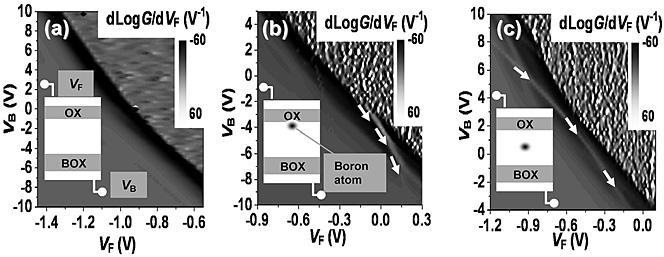
of the channel containing only a few dopant atoms. The conductance G was measured at 6 K. Figure 1 shows the contour plot of dLogG/dVF as a function of the front-gate voltage (VF) and of the substrate back-gate voltage (VB). The conductance modulation, indicated by the arrows, was observed in transistors containing a single boron atom [Figs. 1(b) and (c)] but not in an undoped one [Fig. 1(a)]. These modulations are due to the trapping of a single hole by the boron atom. From the capacitance analysis of the data, we have identified the depth position of the single boron atom as near the front interface (b) and around the middle of the silicon layer (c).
By doing similar analysis using drain bias as a parameter, we will also
be able to obtain information about the dopant’s lateral position, i.e.,
the position along the transport channel, which will lead us to a complete
identification of dopant locations in a nanotransistor.
[1] Y. Ono et al., Appl. Phys. Lett. 90 (2007) 102106.
[2] M. A. H. Khalafalla et al., Appl. Phys. Lett. 91 (2007) 263513.
[3] Y. Ono et al., Appl. Surf. Sci. 254 (2008) 6252.
 |
||
|