Physical Science Laboratory
Three-dimensional (3D) nanostructures are now attracting great interest
because of their possible applications, such as to nanomechanical devices
and nanorobotics. To build various 3D nanostructures, we have devised and
are developing 3D electron beam (EB) lithography (3D-EBL). Although our
technique has some advantages, such as high resolution and fast fabrication,
it has so far shown drawbacks related to the electron scattering/proximity
effect and to the poor precision of structure/3D alignment, compared with
some other 3D fabrication techniques. We have newly devised two methods
in 3D-EBL to significantly improve the 3D alignment and reduce the proximity
effect.
When we make complicated 3D structures with this technique, the EB writes
from largely different directions and therefore should be well positioned
three-dimensionally; high accuracy of 3D alignment is necessary. The high
accuracy is achieved by using a transmission electron image to accurately
control sample rotation (< 1 mrad) and obtain sufficient accuracy of
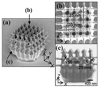
2D positioning of EB writing on a rotated sample [1]. In a 3D nanostructure
we created in negative resist (hydrogen silsesquioxane, HSQ), the 3D alignment
accuracy is on the order of 10 nm (Fig. 1). When we use positive resist,
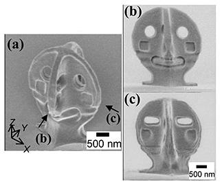
the proximity effect is very serious. However, we have succeeded in suppressing
the proximity effect by leaving buffer areas (not exposed to EB) that surround
the target structure and have sizes similar to the range of fast secondary
electrons. As a result, we have reduced undesirable dissipated energy,
which changes vertically in the resist [2]. Figure 2 shows SEM images of
a 3D nanostructure in positive resist [poly(methyl methacrylate), PMMA],
which demonstrates a high aspect ratio and the great flexibility of structures
that can be created by the technique.
These methods will accelerate the development of 3D-EBL, making it promising for various nanotechnology applications.
This work was supported in part by KAKENHI (20246064).
[1] K. Yamazaki and H. Yamaguchi, J. Vac. Sci. Technol. B 26 (2008) 2529.
[2] K. Yamazaki and H. Yamaguchi, Appl. Phys. Exp. 1 (2008) 098001.
 |
 |
|||||
|
|