Tetsuomi Sogawa*, and Hiroshi Yamaguchi
Physical Science Laboratory, *Optical Science Laboratory
Optically induced dynamic backaction in micromechanical systems has recently
become the focus of research [1, 2]. Cavity-induced opto-mechanical coupling
via radiation pressure or photothermal stress influences the thermal vibration
of the mechanical system, leading to amplification and de-amplification
of the vibration modes [1, 2]. The vibration amplification is of great
interest because it can lead to the self-oscillation of a micromechanical
resonator [1, 2]. The de-amplification is of equal interest because it
enables cooling of the vibration modes [1, 2]. In contrast, we have recently
observed novel opto-mechanical coupling, which does not require any cavities
but is based on optical carrier excitation [3, 4]. Here, we report the
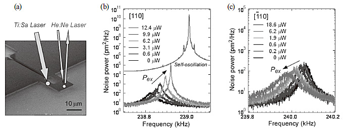
carrier-mediated opto-mechanical coupling found in n-GaAs/i-GaAs bilayer cantilevers [Fig. 1(a)].
The carrier-mediated opto-mechanical coupling is based on the strain-assisted opto-piezoelectric effect, which is associated with the separation of electron-hole pairs due to the built-in electric field. Thermal vibration of the [110]-oriented cantilever is amplified by the optical excitation with the near absorption-edge wavelength (λex = 840 nm at 50 K) and the self-oscillation is induced for the strong excitation (Pex > 10µW) [Fig. 1(b)]. In contrast, for the [-110]-oriented cantilever,
the opto-piezoelectric backaction de-amplifies the vibration because the
piezoelectric effect is reversed in the 90-degree rotated orientation [Fig.
1(c)]. This opto-piezoelectric backaction is maximized when the laser wavelength
matches the optical absorption edge [4]. This is because the strain-induced
change in the optical absorption is maximized at the strain-sensitive absorption
edge. This carrier-mediated opto-mechanical coupling has an advantage in
compatibility with semiconductor opto-electronics and will also provide
a tool for studying the fundamental properties of semiconductors, such
as carrier dynamics, strain effects, and carrier-related energy relaxation.
[1] I. Favero and K. Karrai, Nature Photon. 3 (2009) 201.
[2] C. H. Metzger and K. Karrai, Nature 432 (2004) 1002.
[3] H. Okamoto et al., Appl. Phys. Express. 2 (2009) 035001.
[4] H. Okamoto et al., Phys. Rev. Lett. 106 (2011) 036801.
 |
||
|