Optical Science Laboratory
Semiconductor nanowires (NWs) have attracted much attention because of
their exceptional versatility and potential for a wide range of applications,
from electronics and photonics to biochemistry and medicine [1]. There
are two main approaches to the integration of NW-based devices: (1) using
freestanding NWs epitaxially grown on a patterned substrate; (2) using
an ex-situ assembly method designed to align NWs removed from the grown substrate
and dispersed on another substrate. The former approach is preferable because
of the contamination that occurs during the ex-situ assembly process with
the latter approach. However, a freestanding structure is very difficult
to use as regards electrode formation. The most attractive way to integrate
and extend the applications of NW-based devices is to grow the NWs laterally
on the substrates with an in-situ process. In the current work, we developed
a technique for growing lateral GaAs NWs on GaAs (311)B and (001) substrates
in the vapor-liquid-solid (VLS) growth mode and demonstrated its high controllability
in terms of size, site, and composition [2, 3].
We used Au nanoparticles to catalyze the NW growth in the VLS mode. First,
we investigated lateral GaAs NWs grown on a (311)B substrate under optimized
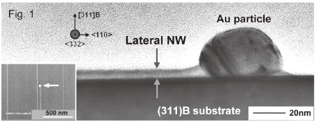
growth conditions in a metalorganic vapor phase epitaxy system. Figure
1 shows a cross-sectional transmission electron microscopy (TEM) image
of a lateral GaAs NW. There is a Au nanoparticle at the tip of the NW,
indicating that the NW is grown in the Au-catalyzed VLS mode. This enables
us to control their size and density by using size- and density-selective
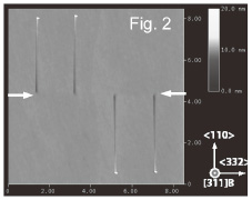
Au colloidal nanoparticles. We grew the site-specific lateral NW array
by using a lithographically defined Au dot array. Figure 2 shows an atomic
force microscopy (AFM) image of the array. To form heterostructures for
bandgap engineering in the lateral NWs, we incorporated indium (In) during
the growth and confirmed the realization of lateral InGaAs NWs [3]. We
expect that the planar NW structure will provide new opportunities and
new functionalities for the development of electronic devices and highly
efficient photonic devices.
[1] L. Samuelson, Mater. Today 6 (2003) 22.
[2] G. Zhang, K. Tateno, H. Gotoh, and H. Nakano, Nanotechnology 21 (2010) 095607.
[3] G. Zhang, K. Tateno, H. Gotoh, and T. Sogawa, Appl. Phys. Express 3 (2010) 105002.
 |
 |
|||||
|
|