Materials Science Laboratory
For graphene, which is a material of great interest for the future electronics,
establishing a method for its wafer-scale fabrication remains a challenge
for its application to largescale integration. We have proposed a new approach
to fabricate graphene based on gassource molecular beam epitaxy (MBE) and
have shown its feasibility [1]. Then, we observed an interesting nanostructure,
which forms a network. Here, we report an investigation of its structural
details [2].
As a substrate, we used graphene, from one to two layers, formed on n-type
SiC(0001) by annealing at 1800ºC in Ar ambient at about 100 Torr.
For the MBE growth, the substrate was heated under the flow of ethanol
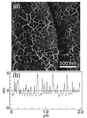
cracked by a W filament set at 2000ºC. By atomic force microscopy
(AFM), the topographic image of a sample grown at 915ºC was obtained
[Fig. 1(a)]. In this image, the network structure can be seen on the substrate
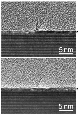
surface. Crosssectional transmission electron microscopy (TEM) images of
this sample in Fig. 2 reveal that these networks consist of one or two
layers of graphene, which stick out from the surface like a fin whose height
is about 5 nm. (Here, we call this ridge-structure a “graphene nanofin”.)
We speculate that the nanofins would be formed by collisions between incommensurate
domains of the laterally growing graphene at their boundary, which means
that a single domain of graphene islands is surrounded by the nanofins.
Thus, the domain size of the laterally grown graphene is estimated to be
less than 100 nm using the average distance between the nanofins from the
section analysis of Fig. 1(b). This fin structure of atomic layer thickness
with an open end has not been reported previously and is observed here
for the first time. We expect that the graphene nanofin could be applied
for interconnection and devices as the thinnest material of one atomic
layer.
This work was supported by KAKENHI.
[1] F. Maeda and H. Hibino, Phys. Status Solidi B 247 (2010) 916.
[2] F. Maeda and H. Hibino, J. Phys. D: Appl. Phys. 44 (2011) 435305.
 |
 |
|||||
|
|