Physical Science Laboratory, *Paul-Drude-Institut
As semiconductor devices become more advanced and more highly integrated,
further miniaturization and further reduction of power consumption are
desired. Atomic-scale devices are the ultimate ones for meeting these demands.
A promising way to construct these devices is to use a scanning probe microscope
system. Up to now, we have achieved vertical manipulation of In atoms on
an InAs(111)A surface by means of reversible tip-surface transfer [1].
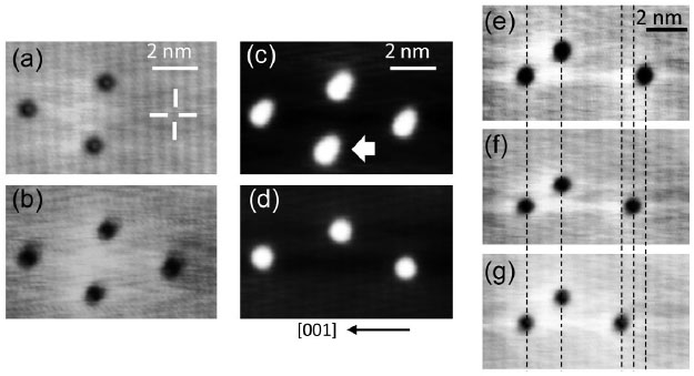
Here we have succeeded manipulation of In atoms in not only vertical but
also horizontal directions on an InAs(110) surface obtained by cleaving
in ultra-high vacuum [2].
On the InAs(111)A surface, the manipulated In atom is bound to the potential
pocket originating from the surface reconstruction resulting in difficulty
for the lateral manipulation. In contrast, on the InAs(110) surface, the
surface reconstruction effect is small and the potential pockets are not
very deep. Taking advantage of inelastic tunneling excitation and inversion
asymmetry of the surface, the In atoms can be manipulated in the specific
horizontal direction ([001]) (Fig. 1).
Many compound semiconductors have same zinc-blend crystal structure as
InAs. Wide and flat (110) surface can be obtained easily by cleaving. On
the basis of our achievement, progress of the atom manipulation on other
semiconductor (110) surfaces and on crosssectional surfaces of heterostructures
is expected.
This work was partly supported by a subsidy from the Strategic Japanese-German
International Cooperative Program on Nanoelectronics supported by the Japan
Science and Technology Agency (JST) and the German Research Foundation
(DFG).
[1] S. Fölsch, J. Yang, C. Nacci, and K. Kanisawa, Phys. Rev. Lett.
103 (2009) 096104.
[2] K. Suzuki, S. Flösch, and K. Kanisawa, Appl. Phys. Express 4 (2011) 085002.
 |
||
|