Physical Science Laboratory, *NTT Photonics Laboratories
Quantum nanostructures, such as quantum point contacts (QPCs) or quantum
dots, in high-In-content InxGa1-xAs offer unique functionalities originated from its material properties.
Firstly, by exploiting the strong spin-orbit interaction (SOI) in InGaAs,
the electronic spin can be manipulated through the SOI. As an example,
electrons moving through QPC experience the selective spin-flipping caused
by SOI induced spin-splitting, which implies that the InGaAs QPC works
as a spin-polarizer without the need of magnetic field [1]. Secondarily,
InGaAs nanostructures are promising for the development of semiconductor/superconductor
hybrid devices. Since high-In-content InxGa1-xAs forms low Schottky barriers (or no barrier for x > 0.77) against most metals, superconducting Cooper pairs can be effectively injected into InGaAs. Superconducting quantum point contact, a counterpart of the semiconducting QPC, has been intensively investigated to realize a quantum bit using Andreev bound states or to observe Majorana fermions that are induced at the interface between an s-wave superconducting electrode and one-dimensional channel with strong SOI.
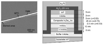
In this study, we improved fabrication technique to realize QPCs in an
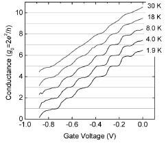
In0.75Ga0.25As/InAlAs two-dimensional electron gas heterostructure [2]. The key challenge in realizing a wellbehaved QPC is efficient electrostatic control of a one-dimensional channel using the gate electrode. The fabricated QPCs employ a 100-nm-wide mesa constriction and a gate electrode that wraps around the constriction for three-dimensional electric-field gating. Conformal aluminum-oxide growth by means of atomic layer deposition is employed to suppress gate leakage while minimizing the interface state density. Figure 1 shows an SEM image of the fabricated QPC and a schematic drawing of the cross-section. The wrap-gate QPCs show clear conductance steps, demonstrating the formation of one-dimensional channels with quantized transverse modes, as shown in Fig. 2. This technique can be easily extended to the fabrication of quantum dots and superconductor/QPC/superconductor junctions, which opens up a novel approach for the studies of spin-related phenomena in InGaAs-based quantum nanostructures.
This work was supported by KAKENHI.
[1] M. Eto et al., J. Phys. Soc. Jpn. 74 (2005) 1934.
[2] H. Irie et al., Appl. Phys. Express 5 (2012) 024001.
 |
 |
|||||
|
|