Eiichi Kuramochi, Hideaki Taniyama, and Masaya Notomi
Optical Science Laboratory
Slow light (SL) in an optical chip provides an enhanced light-matter interaction, thanks to the longitudinally compressed optical field and the prolonged interaction time between the medium and the slowly-propagating light within. We have already fabricated high-bandwidth SL waveguides using a 1-D chain of silicon photonic-crystal ultrahigh-Q (〜1 million) nanocavities and demonstrated vg less than c/100 in the telecom band [1]. This time we demonstrated SL
enhancement of all-optical wavelength-conversion efficiency in our device
via the four-wave-mixing (FWM) experiment [2].
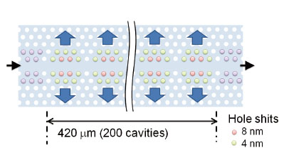
Schematic of our SL waveguide (γ = c/36, 0.42-mm long) is shown in Fig. 1. We input telecom-band pump and
signal beam into the device and observed a new idler field that was created
by the stimulated FWM, which arises from the third-order optical nonlinearity
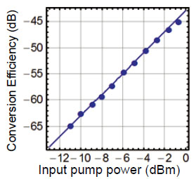
in the core material (Si). We plotted measured signal-to-idler wavelength
conversion efficiency as a function of input pump power as shown in Fig.
2. The conversion efficiency was proportional to the the square of the
pump power because the FWM is a two-photon absorption process. From the
result, we obtained the value of nonlinear constant γ , which is the degree of waveguide nonlinearity, as 18,600 /W/m. The value is 107 times larger than that of standard single-mode fibers and even larger than 300 /W/m of a silicon wire waveguide (vg = c/4.2) [3] and 2,930 /W/m of a photonic crystal SL waveguide that employed
a line defect mode (vg = c/30) [4]. The extremely high nonlinearity of our device is originating
from SL enhancement ((1/vg)2 dependence of γ ) and a strong spatial confinement of the SL mode due to wavelengthsized photonic crystal cavities. This value is the highest yet reported for silicon-core nonlinear waveguides with an integrated structure, indicating a potential to provide a new stage for integrated waveguide photonic devices with ultralow power consumption.
This work was supported by KAKENHI.
[1] M. Notomi, E. Kuramochi, and T. Tanabe, Nature Photon. 2 (2008) 741.
[2] N. Matsuda et al., Opt. Express 19 (2011) 19861.
[3] K. Harada et al., IEEE J. Sel. Top. Quantum Electron. 16 (2010) 325.
[4] C. Monat et al., IEEE. J. Sel. Top. Quantum Electron. 16 (2010) 344.
 |
 |
|||||
|
|